This article needs additional citations for verification .(December 2024) |
Xetal is the name of a family of non-commercial massively parallel processors developed within Philips Research.
This article needs additional citations for verification .(December 2024) |
Xetal is the name of a family of non-commercial massively parallel processors developed within Philips Research.
The Xetal was conceived in 1999 at Philips Research when researchers Kleihorst, Abbo and Van der Avoird investigated possibilities for combining a CMOS image sensor with powerful image processing logic. Since CMOS image sensors (contrary to CCD sensors) can be produced using the same manufacturing process as processors, both could be combined in a single integrated circuit (IC). With the image sensor and image processing combined on the same die, it is essentially possible to parallelize image processing up to the level where each pixel has its dedicated image processing logic. In such a design the image sensor would be in the upper layers of the IC while the image processing would be done in the lower layers, so image data would be transferred from one layer to the other, instead of through external pins or wires. Additionally there is inherent parallelism in image processing algorithms. Many algorithms do the same processing on every pixel. Image processing is therefore a suitable domain for a massively parallel approach using an SIMD architecture. Although massive parallelism is not a new idea (earlier examples include ILLIAC IV and Goodyear MPP) the Xetal 1 was one of the first to apply this approach to image processing.
The first design combined a QVGA image sensor with line-based A/D conversion. In this design, the analogue pixel values of the sensor were converted line by line (instead of pixel by pixel). For every line there were 320 A/D converters. Each A/D converter is connected to a dedicated processing element (PE) to do image processing. This parallel design meant that a complete line of 320 pixels could essentially be processed in a single clock cycle. This parallelism was also applied to the memory architecture, where each processing element could access a pixel from a so-called /Line memory. Simulations of this design showed that the digital (PE) part of the chip caused noise on the A/D converters. On top of that CMOS sensors at the time were produced using a 350-nm process using 3 metal layers. Few layers were used so as to limit height variations in the sensor surface which could cause artifacts. For discrete logic the 180-nm process was more common. Also, more layers were used. Development of the CMOS sensor and the image processor therefore continued independently.
The image processor resulting from this was the Xetal 1, first produced in 2001. It was manufactured using a 180-nm process and was designed to run at 18 MHz with 320 PEs and 16 line memories. Since each of the PEs can perform one operation per clock cycle, the raw performance at this clock speed is 5.7 GOPS (109 operations per second). As a result, combined with a CMOS image sensor at QVGA resolution running at 15 frames per second, the Xetal 1 could essentially perform 5000 operations per pixel. During testing it turned out the Xetal 1 could even be clocked up to 38 MHz, more than double the original specification, resulting in a raw performance of over 12 GOPS. Moreover, it achieved this performance at very low power consumption (1–2 Watt). It was soon discovered that with these levels of performance it was possible to do much more than just image processing. The research team which now also involved Ben Schueler, Joost 't Hart, Peter Meijer, Alexander Danilin, Xinting Chao and Herman Budde created demonstrations which showed that Xetal 1 was capable of running computer vision algorithms such as object recognition and tracking, including a self-playing pinball machine, air drumming, and Robocup robots. A compiler was made by Sebastian Mouy and Joost 't Hart. Usually the Xetal-I chip was shown as a wireless smart camera named WiCa, a design by Schueler.
Xetal-I was later succeeded by the Xetal-II chip. The project was stopped at NXP around 2008 because the company decided not to pursue in systems on chip.

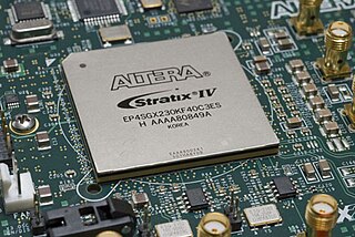
A field-programmable gate array (FPGA) is a type of configurable integrated circuit that can be repeatedly programmed after manufacturing. FPGAs are a subset of logic devices referred to as programmable logic devices (PLDs). They consist of an array of programmable logic blocks with a connecting grid, that can be configured "in the field" to interconnect with other logic blocks to perform various digital functions. FPGAs are often used in limited (low) quantity production of custom-made products, and in research and development, where the higher cost of individual FPGAs is not as important, and where creating and manufacturing a custom circuit wouldn't be feasible. Other applications for FPGAs include the telecommunications, automotive, aerospace, and industrial sectors, which benefit from their flexibility, high signal processing speed, and parallel processing abilities.

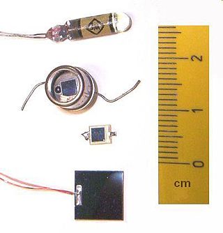
A photodiode is a semiconductor diode sensitive to photon radiation, such as visible light, infrared or ultraviolet radiation, X-rays and gamma rays. It produces an electrical current when it absorbs photons. This can be used for detection and measurement applications, or for the generation of electrical power in solar cells. Photodiodes are used in a wide range of applications throughout the electromagnetic spectrum from visible light photocells to gamma ray spectrometers.

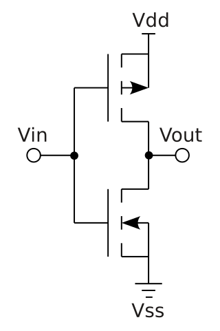
Complementary metal–oxide–semiconductor is a type of metal–oxide–semiconductor field-effect transistor (MOSFET) fabrication process that uses complementary and symmetrical pairs of p-type and n-type MOSFETs for logic functions. CMOS technology is used for constructing integrated circuit (IC) chips, including microprocessors, microcontrollers, memory chips, and other digital logic circuits. CMOS technology is also used for analog circuits such as image sensors, data converters, RF circuits, and highly integrated transceivers for many types of communication.

In electronics and especially synchronous digital circuits, a clock signal is an electronic logic signal which oscillates between a high and a low state at a constant frequency and is used like a metronome to synchronize actions of digital circuits. In a synchronous logic circuit, the most common type of digital circuit, the clock signal is applied to all storage devices, flip-flops and latches, and causes them all to change state simultaneously, preventing race conditions.

A Bayer filter mosaic is a color filter array (CFA) for arranging RGB color filters on a square grid of photosensors. Its particular arrangement of color filters is used in most single-chip digital image sensors used in digital cameras, and camcorders to create a color image. The filter pattern is half green, one quarter red and one quarter blue, hence is also called BGGR, RGBG, GRBG, or RGGB.
Silicon on sapphire (SOS) is a hetero-epitaxial process for metal–oxide–semiconductor (MOS) integrated circuit (IC) manufacturing that consists of a thin layer of silicon grown on a sapphire wafer. SOS is part of the silicon-on-insulator (SOI) family of CMOS technologies.
The R420 GPU, developed by ATI Technologies, was the company's basis for its 3rd-generation DirectX 9.0/OpenGL 2.0-capable graphics cards. Used first on the Radeon X800, the R420 was produced on a 0.13 micrometer low-K photolithography process and used GDDR-3 memory. The chip was designed for AGP graphics cards.

A mixed-signal integrated circuit is any integrated circuit that has both analog circuits and digital circuits on a single semiconductor die. Their usage has grown dramatically with the increased use of cell phones, telecommunications, portable electronics, and automobiles with electronics and digital sensors.

An image sensor or imager is a sensor that detects and conveys information used to form an image. It does so by converting the variable attenuation of light waves into signals, small bursts of current that convey the information. The waves can be light or other electromagnetic radiation. Image sensors are used in electronic imaging devices of both analog and digital types, which include digital cameras, camera modules, camera phones, optical mouse devices, medical imaging equipment, night vision equipment such as thermal imaging devices, radar, sonar, and others. As technology changes, electronic and digital imaging tends to replace chemical and analog imaging.

An active-pixel sensor (APS) is an image sensor, which was invented by Peter J.W. Noble in 1968, where each pixel sensor unit cell has a photodetector and one or more active transistors. In a metal–oxide–semiconductor (MOS) active-pixel sensor, MOS field-effect transistors (MOSFETs) are used as amplifiers. There are different types of APS, including the early NMOS APS and the now much more common complementary MOS (CMOS) APS, also known as the CMOS sensor. CMOS sensors are used in digital camera technologies such as cell phone cameras, web cameras, most modern digital pocket cameras, most digital single-lens reflex cameras (DSLRs), mirrorless interchangeable-lens cameras (MILCs), and lensless imaging for cells.

In digital imaging, a color filter array (CFA), or color filter mosaic (CFM), is a mosaic of tiny color filters placed over the pixel sensors of an image sensor to capture color information.
The asynchronous array of simple processors (AsAP) architecture comprises a 2-D array of reduced complexity programmable processors with small scratchpad memories interconnected by a reconfigurable mesh network. AsAP was developed by researchers in the VLSI Computation Laboratory (VCL) at the University of California, Davis and achieves high performance and energy efficiency, while using a relatively small circuit area. It was made in 2006.
OmniVision Technologies Inc. is an American subsidiary of Chinese semiconductor device and mixed-signal integrated circuit design house Will Semiconductor. The company designs and develops digital imaging products for use in mobile phones, laptops, netbooks webcams, security, entertainment, automotive and medical imaging systems. Headquartered in Santa Clara, California, OmniVision Technologies has offices in the US, Western Europe and Asia.
Intrinsity was a privately held Austin, Texas based fabless semiconductor company; it was founded in 1997 as EVSX on the remnants of Exponential Technology and changed its name to Intrinsity in 2000. It had around 100 employees and supplied tools and services for highly efficient semiconductor logic design, enabling high performance microprocessors with fewer transistors and low power consumption. The acquisition of the firm by Apple Inc. was confirmed on April 27, 2010.

Exmor is a technology developed by Sony and implemented on some of their CMOS image sensors. It performs on-chip analog/digital signal conversion and two-step noise reduction in parallel on each column of the CMOS sensor.
A massively parallel processor array, also known as a multi purpose processor array (MPPA) is a type of integrated circuit which has a massively parallel array of hundreds or thousands of CPUs and RAM memories. These processors pass work to one another through a reconfigurable interconnect of channels. By harnessing a large number of processors working in parallel, an MPPA chip can accomplish more demanding tasks than conventional chips. MPPAs are based on a software parallel programming model for developing high-performance embedded system applications.

A back-illuminated sensor, also known as backside illumination (BI) sensor, is a type of digital image sensor that uses a novel arrangement of the imaging elements to increase the amount of light captured and thereby improve low-light performance.

The Nikon Expeed image/video processors are media processors for Nikon's digital cameras. They perform a large number of tasks: Bayer filtering, demosaicing, image sensor corrections/dark-frame subtraction, image noise reduction, image sharpening, image scaling, gamma correction, image enhancement/Active D-Lighting, colorspace conversion, chroma subsampling, framerate conversion, lens distortion/chromatic aberration correction, image compression/JPEG encoding, video compression, display/video interface driving, digital image editing, face detection, audio processing/compression/encoding and computer data storage/data transmission.
An oversampled binary image sensor is an image sensor with non-linear response capabilities reminiscent of traditional photographic film. Each pixel in the sensor has a binary response, giving only a one-bit quantized measurement of the local light intensity. The response function of the image sensor is non-linear and similar to a logarithmic function, which makes the sensor suitable for high dynamic range imaging.
In parallel computing, granularity of a task is a measure of the amount of work which is performed by that task.