Buffer amplifier

Last updated
Figure 1: Ideal voltage buffer (top) and current buffer (bottom) Ideal Buffers.svg
Figure 1: Ideal voltage buffer (top) and current buffer (bottom)

In electronics, a buffer amplifier is a unity gain amplifier that copies a signal from one circuit to another while transforming its electrical impedance to provide a more ideal source (with a lower output impedance for a voltage buffer or a higher output impedance for a current buffer). This "buffers" the signal source in the first circuit against being affected by currents from the electrical load of the second circuit and may simply be called a buffer or follower when context is clear.

Contents

Voltage buffer

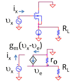
A voltage buffer amplifier is used to transform a voltage signal with high output impedance from a first circuit into an identical voltage with low impedance for a second circuit. The interposed buffer amplifier prevents the second circuit from loading the first circuit unacceptably and interfering with its desired operation, since without the voltage buffer, the voltage of the second circuit is influenced by output impedance of the first circuit (as it is larger than the input impedance of the second circuit). In the ideal voltage buffer (Figure 1 top), the input impedance is infinite and the output impedance is zero. Other properties of the ideal buffer are: perfect linearity, regardless of signal amplitudes; and instant output response, regardless of the speed of the input signal.

If the voltage is transferred unchanged (the voltage gain Av is 1), the amplifier is a unity gain buffer; also known as a voltage follower because the output voltage follows or tracks the input voltage. Although the voltage gain of a voltage buffer amplifier may be (approximately) unity, it usually provides considerable current gain and thus power gain. However, it is commonplace to say that it has a gain of 1 (or the equivalent 0  dB), referring to the voltage gain.

As an example, consider a Thévenin source (voltage VA, series resistance RA) driving a resistor load RL. Because of voltage division (also referred to as "loading") the voltage across the load is only VA RL/RL + RA. However, if the Thévenin source drives a unity gain buffer such as that in Figure 1 (top, with unity gain), the voltage input to the amplifier is VA, and with no voltage division because the amplifier input resistance is infinite. At the output the dependent voltage source delivers voltage Av VA = VA to the load, again without voltage division because the output resistance of the buffer is zero. A Thévenin equivalent circuit of the combined original Thévenin source and the buffer is an ideal voltage source VA with zero Thévenin resistance.

Current buffer

Typically a current buffer amplifier is used to transform a current signal with a low output impedance from a first circuit into an identical current with high impedance for a second circuit. [1] The interposed buffer amplifier prevents the second circuit from loading the first circuit's current unacceptably and interfering with its desired operation. In the ideal current buffer (Figure 1 bottom), the output impedance is infinite (an ideal current source) and the input impedance is zero (a short circuit). Again, other properties of the ideal buffer are: perfect linearity, regardless of signal amplitudes; and instant output response, regardless of the speed of the input signal.

For a current buffer, if the current is transferred unchanged (the current gain βi is 1), the amplifier is again a unity gain buffer; this time known as a current follower because the output current follows or tracks the input current.

As an example, consider a Norton source (current IA, parallel resistance RA) driving a resistor load RL. Because of current division (also referred to as "loading") the current delivered to the load is only IA RA/RL + RA. However, if the Norton source drives a unity gain buffer such as that in Figure 1 (bottom, with unity gain), the current input to the amplifier is IA, with no current division because the amplifier input resistance is zero. At the output the dependent current source delivers current βi IA = IA to the load, again without current division because the output resistance of the buffer is infinite. A Norton equivalent circuit of the combined original Norton source and the buffer is an ideal current source IA with infinite Norton resistance.

Voltage buffer examples

Op-amp implementation

Figure 2: A negative feedback amplifier Block Diagram for Feedback.svg
Figure 2: A negative feedback amplifier
Figure 3. An op-amp-based unity gain buffer amplifier Op-Amp Unity-Gain Buffer.svg
Figure 3. An op-amp–based unity gain buffer amplifier
A voltage follower boosted by a transistor; also can be seen as the "ideal transistor" without a base-emitter forward bias voltage drop on the input signal. This is the basic circuit of linear voltage regulators Voltage follwer boosted 4clamp II.svg
A voltage follower boosted by a transistor; also can be seen as the "ideal transistor" without a base-emitter forward bias voltage drop on the input signal. This is the basic circuit of linear voltage regulators

A unity gain buffer amplifier may be constructed by applying a full series negative feedback (Fig. 2) to an op-amp simply by connecting its output to its inverting input, and connecting the signal source to the non-inverting input (Fig. 3). Unity gain here implies a voltage gain of one (i.e. 0 dB), but significant current gain is expected. In this configuration, the entire output voltage (β = 1 in Fig. 2) is fed back into the inverting input. The difference between the non-inverting input voltage and the inverting input voltage is amplified by the op-amp. This connection forces the op-amp to adjust its output voltage to simply equal the input voltage (Vout follows Vin so the circuit is named op-amp voltage follower).

The impedance of this circuit does not come from any change in voltage, but from the input and output impedances of the op-amp. The input impedance of the op-amp is very high (1 to 10 ), meaning that the input of the op-amp does not load down the source and draws only minimal current from it. Because the output impedance of the op-amp is very low, it drives the load as if it were a perfect voltage source. Both the connections to and from the buffer are therefore bridging connections, which reduce power consumption in the source, distortion from overloading, crosstalk and other electromagnetic interference.

Simple transistor circuits

Figure 4: Top: BJT voltage follower Bottom: Small-signal, low-frequency equivalent circuit using hybrid-pi model Bipolar Voltage Follower.png
Figure 4: Top: BJT voltage follower Bottom: Small-signal, low-frequency equivalent circuit using hybrid-pi model
Figure 5: Top: MOSFET voltage follower Bottom: Small-signal, low-frequency equivalent circuit using hybrid-pi model MOSFET Voltage Follower.png
Figure 5: Top: MOSFET voltage follower Bottom: Small-signal, low-frequency equivalent circuit using hybrid-pi model

Other unity gain buffer amplifiers include the bipolar junction transistor in common-collector configuration (called an emitter follower because the emitter voltage follows the base voltage, or a voltage follower because the output voltage follows the input voltage); the field effect transistor in common-drain configuration (called a source follower because the source voltage follows the gate voltage or, again, a voltage follower because the output voltage follows the input voltage); or similar configurations using vacuum tubes (cathode follower), or other active devices. All such amplifiers actually have a gain of slightly less than unity (though the loss may be small and unimportant) and add a DC offset. Only one transistor is shown as the active device in these schematics (however, the current source these circuits may require transistors too).

Impedance transformation using the bipolar voltage follower

Using the small-signal circuit in Figure 4, the impedance seen looking into the circuit is

(The analysis uses the relation gmrπ = (IC /VT) (VT /IB) = β, which follows from the evaluation of these parameters in terms of the bias currents.) Assuming the usual case where rO >> RL, the impedance looking into the buffer is larger than the load RL without the buffer by a factor of (β + 1), which is substantial because β is large. The impedance is increased even more by the added rπ, but often rπ << (β + 1) RL, so the addition does not make much difference

Impedance transformation using the MOSFET voltage follower

Using the small-signal circuit in Figure 5, the impedance seen looking into the circuit is no longer RL but instead is infinite (at low frequencies) because the MOSFET draws no current.

As frequency is increased, the parasitic capacitances of the transistors come into play and the transformed input impedance drops with frequency.

Chart of single-transistor amplifiers

Some configurations of single-transistor amplifier can be used as a buffer to isolate the driver from the load. For most digital applications, an NMOS voltage follower (common drain) is the preferred configuration.[ dubious ] These amplifiers have high input impedance, which means that the digital system will not need to supply a large current.

Amplifier typeMOSFET (NMOS)BJT    (npn)   Notes
Common gate/base N-channel JFET common gate.svg NPN common base.svg Typically used for current buffering
Common drain/collector N-channel JFET source follower.svg NPN emitter follower.svg Voltage gain is close to unity, used for voltage buffering.

Logic buffer amplifiers

A non-linear buffer amplifier is sometimes used in digital circuits where a high current is required, perhaps for driving more gates than the normal fan-out of the logic family used, or for driving displays, or long wires, or other difficult loads. It is common for a single package to contain several discrete buffer amplifiers. For example, a hex buffer is a single package containing 6 buffer amplifiers, and an octal buffer is a single package containing 8 buffer amplifiers. The terms inverting buffer and non-inverting buffer effectively correspond with high-current capability single-input NOR or OR gates respectively.

Speaker array amplifiers

The majority of amplifiers used to drive large speaker arrays, such as those used for rock concerts, are amplifiers with 26-36dB voltage gain capable of high amounts of current into low impedance speaker arrays where the speakers are wired in parallel.

Driven guards

A driven guard utilizes a voltage buffer to protect a very high impedance signal line by surrounding the line with a shield driven by a buffer to the same voltage as the line, the close voltage matching of the buffer prevents the shield from leaking significant current into the high impedance line while the low impedance of the shield can absorb any stray currents that could affect the signal line.

Current buffer examples

Simple unity gain buffer amplifiers include the bipolar junction transistor in common-base configuration, or the MOSFET in common-gate configuration (called a current follower because the output current follows the input current). The current gain of a current buffer amplifier is (approximately) unity.

Simple transistor circuits

Figure 6: Bipolar current follower biased by current source IE and with active load IC Bipolar current follower2.PNG
Figure 6: Bipolar current follower biased by current source IE and with active load IC

Figure 6 shows a bipolar current buffer biased with a current source (designated IE for DC emitter current) and driving another DC current source as active load (designated IC for DC collector current). The AC input signal current iin is applied to the emitter node of the transistor by an AC Norton current source with Norton resistance RS. The AC output current iout is delivered by the buffer via a large coupling capacitor to load RL. This coupling capacitor is large enough to be a short circuit at frequencies of interest.

Because the transistor output resistance connects input and output sides of the circuit, there is a (very small) backward voltage feedback from the output to the input so this circuit is not unilateral. In addition, for the same reason, the input resistance depends (slightly) upon the output load resistance, and the output resistance depends significantly on the input driver resistance. For more detail see the article on common base amplifier.

See also

Related Research Articles

<span class="mw-page-title-main">Amplifier</span> Electronic device/component that increases the strength of a signal

An amplifier, electronic amplifier or (informally) amp is an electronic device that can increase the magnitude of a signal. It is a two-port electronic circuit that uses electric power from a power supply to increase the amplitude of a signal applied to its input terminals, producing a proportionally greater amplitude signal at its output. The amount of amplification provided by an amplifier is measured by its gain: the ratio of output voltage, current, or power to input. An amplifier is defined as a circuit that has a power gain greater than one.

<span class="mw-page-title-main">Operational amplifier</span> High-gain voltage amplifier with a differential input

An operational amplifier is a DC-coupled high-gain electronic voltage amplifier with a differential input and, usually, a single-ended output. In this configuration, an op amp produces an output potential that is typically 100,000 times larger than the potential difference between its input terminals. The operational amplifier traces its origin and name to analog computers, where they were used to perform mathematical operations in linear, non-linear, and frequency-dependent circuits.

<span class="mw-page-title-main">Negative-feedback amplifier</span> Type of electronic amplifier

A negative-feedback amplifier is an electronic amplifier that subtracts a fraction of its output from its input, so that negative feedback opposes the original signal. The applied negative feedback can improve its performance and reduces sensitivity to parameter variations due to manufacturing or environment. Because of these advantages, many amplifiers and control systems use negative feedback.

<span class="mw-page-title-main">Common base</span>

In electronics, a common-base amplifier is one of three basic single-stage bipolar junction transistor (BJT) amplifier topologies, typically used as a current buffer or voltage amplifier.

<span class="mw-page-title-main">Differential amplifier</span> Electrical circuit component which amplifies the difference of two analog signals

A differential amplifier is a type of electronic amplifier that amplifies the difference between two input voltages but suppresses any voltage common to the two inputs. It is an analog circuit with two inputs and and one output , in which the output is ideally proportional to the difference between the two voltages:

<span class="mw-page-title-main">Schmitt trigger</span> Electronic comparator circuit with hysteresis

In electronics, a Schmitt trigger is a comparator circuit with hysteresis implemented by applying positive feedback to the noninverting input of a comparator or differential amplifier. It is an active circuit which converts an analog input signal to a digital output signal. The circuit is named a trigger because the output retains its value until the input changes sufficiently to trigger a change. In the non-inverting configuration, when the input is higher than a chosen threshold, the output is high. When the input is below a different (lower) chosen threshold the output is low, and when the input is between the two levels the output retains its value. This dual threshold action is called hysteresis and implies that the Schmitt trigger possesses memory and can act as a bistable multivibrator. There is a close relation between the two kinds of circuits: a Schmitt trigger can be converted into a latch and a latch can be converted into a Schmitt trigger.

<span class="mw-page-title-main">Common emitter</span> Type of electronic amplifier using a bipolar junction transistor

In electronics, a common-emitter amplifier is one of three basic single-stage bipolar-junction-transistor (BJT) amplifier topologies, typically used as a voltage amplifier. It offers high current gain, medium input resistance and a high output resistance. The output of a common emitter amplifier is inverted; i.e. for a sine wave input signal, the output signal is 180 degrees out of phase with respect to the input.

<span class="mw-page-title-main">Common collector</span> Type of transistor amplifier

In electronics, a common collector amplifier is one of three basic single-stage bipolar junction transistor (BJT) amplifier topologies, typically used as a voltage buffer.

<span class="mw-page-title-main">Input impedance</span> Measure of the opposition to current flow by an external electrical load

In electrical engineering, the input impedance of an electrical network is the measure of the opposition to current (impedance), both static (resistance) and dynamic (reactance), into a load network that is external to the electrical source network. The input admittance is a measure of the load network's propensity to draw current. The source network is the portion of the network that transmits power, and the load network is the portion of the network that consumes power.

<span class="mw-page-title-main">Current source</span> Electronic circuit which delivers or absorbs electric current regardless of voltage

A current source is an electronic circuit that delivers or absorbs an electric current which is independent of the voltage across it.

<span class="mw-page-title-main">Common gate</span> Electronic amplifier circuit type

In electronics, a common-gate amplifier is one of three basic single-stage field-effect transistor (FET) amplifier topologies, typically used as a current buffer or voltage amplifier. In this circuit, the source terminal of the transistor serves as the input, the drain is the output, and the gate is connected to some DC biasing voltage, or "common," hence its name. The analogous bipolar junction transistor circuit is the common-base amplifier.

In electronics, a common-drain amplifier, also known as a source follower, is one of three basic single-stage field-effect transistor (FET) amplifier topologies, typically used as a voltage buffer. In this circuit (NMOS) the gate terminal of the transistor serves as the signal input, the source is the output, and the drain is common to both, hence its name. Because of its low dependence on the load resistor on the voltage gain, it can be used to drive low resistance loads, such as a speaker. The analogous bipolar junction transistor circuit is the common-collector amplifier. This circuit is also commonly called a "stabilizer".

The cascode is a two-stage amplifier that consists of a common-emitter stage feeding into a common-base stage.

This article illustrates some typical operational amplifier applications. A non-ideal operational amplifier's equivalent circuit has a finite input impedance, a non-zero output impedance, and a finite gain. A real op-amp has a number of non-ideal features as shown in the diagram, but here a simplified schematic notation is used, many details such as device selection and power supply connections are not shown. Operational amplifiers are optimised for use with negative feedback, and this article discusses only negative-feedback applications. When positive feedback is required, a comparator is usually more appropriate. See Comparator applications for further information.

In electronics, the Miller effect accounts for the increase in the equivalent input capacitance of an inverting voltage amplifier due to amplification of the effect of capacitance between the input and output terminals. The virtually increased input capacitance due to the Miller effect is given by

<span class="mw-page-title-main">Operational transconductance amplifier</span>

The operational transconductance amplifier (OTA) is an amplifier whose differential input voltage produces an output current. Thus, it is a voltage controlled current source (VCCS). There is usually an additional input for a current to control the amplifier's transconductance. The OTA is similar to a standard operational amplifier in that it has a high impedance differential input stage and that it may be used with negative feedback.

The Miller theorem refers to the process of creating equivalent circuits. It asserts that a floating impedance element, supplied by two voltage sources connected in series, may be split into two grounded elements with corresponding impedances. There is also a dual Miller theorem with regards to impedance supplied by two current sources connected in parallel. The two versions are based on the two Kirchhoff's circuit laws.

<span class="mw-page-title-main">Transimpedance amplifier</span> Amplifier that converts current to voltage

In electronics, a transimpedance amplifier (TIA) is a current to voltage converter, almost exclusively implemented with one or more operational amplifiers. The TIA can be used to amplify the current output of Geiger–Müller tubes, photo multiplier tubes, accelerometers, photo detectors and other types of sensors to a usable voltage. Current to voltage converters are used with sensors that have a current response that is more linear than the voltage response. This is the case with photodiodes where it is not uncommon for the current response to have better than 1% nonlinearity over a wide range of light input. The transimpedance amplifier presents a low impedance to the photodiode and isolates it from the output voltage of the operational amplifier. In its simplest form a transimpedance amplifier has just a large valued feedback resistor, Rf. The gain of the amplifier is set by this resistor and because the amplifier is in an inverting configuration, has a value of -Rf. There are several different configurations of transimpedance amplifiers, each suited to a particular application. The one factor they all have in common is the requirement to convert the low-level current of a sensor to a voltage. The gain, bandwidth, as well as current and voltage offsets change with different types of sensors, requiring different configurations of transimpedance amplifiers.

<span class="mw-page-title-main">Current-feedback operational amplifier</span>

The current-feedback operational amplifier is a type of electronic amplifier whose inverting input is sensitive to current, rather than to voltage as in a conventional voltage-feedback operational amplifier (VFA). The CFA was invented by David Nelson at Comlinear Corporation, and first sold in 1982 as a hybrid amplifier, the CLC103. An early patent covering a CFA is U.S. Patent 4,502,020, David Nelson and Kenneth Saller. The integrated circuit CFAs were introduced in 1987 by both Comlinear and Elantec. They are usually produced with the same pin arrangements as VFAs, allowing the two types to be interchanged without rewiring when the circuit design allows. In simple configurations, such as linear amplifiers, a CFA can be used in place of a VFA with no circuit modifications, but in other cases, such as integrators, a different circuit design is required. The classic four-resistor differential amplifier configuration also works with a CFA, but the common-mode rejection ratio is poorer than that from a VFA.

<span class="mw-page-title-main">Diamond buffer</span>

The diamond buffer or diamond follower is a four-transistor, two-stage, push-pull, translinear emitter follower, or less commonly source follower, in which the input transistors are folded, or placed upside-down with respect to the output transistors. Like any unity buffer, the diamond buffer does not alter the phase and magnitude of input voltage signal; its primary purpose is to interface a high-impedance voltage source with a low-impedance, high-current load. Unlike the more common compound emitter follower, where each input transistor drives the output transistor of the same polarity, each input transistor of a diamond buffer drives the output transistor of the opposite polarity. When the transistors operate in close thermal contact, the input transistors stabilize the idle current of the output pair, eliminating the need for a bias spreader.

References

  1. "Lecture 20 - Transistor Amplifiers (II) - Other Amplifier Stages" (PDF). A current buffer takes the input current which may have a relatively small Norton resistance and replicates the current at the output port, which has a high output resistance ... Input resistance is low ... Output resistance is high ... transform a current source with medium source resistance to an equal current with high source resistance