Related Research Articles
A complex instruction set computer is a computer architecture in which single instructions can execute several low-level operations or are capable of multi-step operations or addressing modes within single instructions. The term was retroactively coined in contrast to reduced instruction set computer (RISC) and has therefore become something of an umbrella term for everything that is not RISC, where the typical differentiating characteristic is that most RISC designs use uniform instruction length for almost all instructions, and employ strictly separate load and store instructions.

Static random-access memory is a type of random-access memory (RAM) that uses latching circuitry (flip-flop) to store each bit. SRAM is volatile memory; data is lost when power is removed.
The Pentium Pro is a sixth-generation x86 microprocessor developed and manufactured by Intel and introduced on November 1, 1995. It introduced the P6 microarchitecture and was originally intended to replace the original Pentium in a full range of applications. Later, it was reduced to a more narrow role as a server and high-end desktop processor. The Pentium Pro was also used in supercomputers, most notably ASCI Red, which used two Pentium Pro CPUs on each computing nodes and was the first computer to reach over one teraFLOPS in 1996, holding the number one spot in the TOP500 list from 1997 to 2000.

Processor power dissipation or processing unit power dissipation is the process in which computer processors consume electrical energy, and dissipate this energy in the form of heat due to the resistance in the electronic circuits.
Bus snooping or bus sniffing is a scheme by which a coherency controller (snooper) in a cache monitors or snoops the bus transactions, and its goal is to maintain a cache coherency in distributed shared memory systems. This scheme was introduced by Ravishankar and Goodman in 1983, under the name "write-once" cache coherency. A cache containing a coherency controller (snooper) is called a snoopy cache.
The Lempel–Ziv–Markov chain algorithm (LZMA) is an algorithm used to perform lossless data compression. It has been under development since either 1996 or 1998 by Igor Pavlov and was first used in the 7z format of the 7-Zip archiver. This algorithm uses a dictionary compression scheme somewhat similar to the LZ77 algorithm published by Abraham Lempel and Jacob Ziv in 1977 and features a high compression ratio and a variable compression-dictionary size, while still maintaining decompression speed similar to other commonly used compression algorithms.
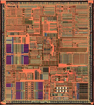
A CPU cache is a hardware cache used by the central processing unit (CPU) of a computer to reduce the average cost to access data from the main memory. A cache is a smaller, faster memory, located closer to a processor core, which stores copies of the data from frequently used main memory locations. Most CPUs have a hierarchy of multiple cache levels, with different instruction-specific and data-specific caches at level 1. The cache memory is typically implemented with static random-access memory (SRAM), in modern CPUs by far the largest part of them by chip area, but SRAM is not always used for all levels, or even any level, sometimes some latter or all levels are implemented with eDRAM.

In electronics, computer science and computer engineering, microarchitecture, also called computer organization and sometimes abbreviated as µarch or uarch, is the way a given instruction set architecture (ISA) is implemented in a particular processor. A given ISA may be implemented with different microarchitectures; implementations may vary due to different goals of a given design or due to shifts in technology.

The RISC Single Chip, or RSC, is a single-chip microprocessor developed and fabricated by International Business Machines (IBM). The RSC was a feature-reduced single-chip implementation of the POWER1, a multi-chip central processing unit (CPU) which implemented the POWER instruction set architecture (ISA). It was used in entry-level workstation models of the IBM RS/6000 family, such as the Model 220 and 230.
The P6 microarchitecture is the sixth-generation Intel x86 microarchitecture, implemented by the Pentium Pro microprocessor that was introduced in November 1995. It is frequently referred to as i686. It was planned to be succeeded by the NetBurst microarchitecture used by the Pentium 4 in 2000, but was revived for the Pentium M line of microprocessors. The successor to the Pentium M variant of the P6 microarchitecture is the Core microarchitecture which in turn is also derived from P6.

The R10000, code-named "T5", is a RISC microprocessor implementation of the MIPS IV instruction set architecture (ISA) developed by MIPS Technologies, Inc. (MTI), then a division of Silicon Graphics, Inc. (SGI). The chief designers are Chris Rowen and Kenneth C. Yeager. The R10000 microarchitecture is known as ANDES, an abbreviation for Architecture with Non-sequential Dynamic Execution Scheduling. The R10000 largely replaces the R8000 in the high-end and the R4400 elsewhere. MTI was a fabless semiconductor company; the R10000 was fabricated by NEC and Toshiba. Previous fabricators of MIPS microprocessors such as Integrated Device Technology (IDT) and three others did not fabricate the R10000 as it was more expensive to do so than the R4000 and R4400.

Error correction code memory is a type of computer data storage that uses an error correction code (ECC) to detect and correct n-bit data corruption which occurs in memory.

The Alpha 21064 is a microprocessor developed and fabricated by Digital Equipment Corporation that implemented the Alpha instruction set architecture (ISA). It was introduced as the DECchip 21064 before it was renamed in 1994. The 21064 is also known by its code name, EV4. It was announced in February 1992 with volume availability in September 1992. The 21064 was the first commercial implementation of the Alpha ISA, and the first microprocessor from Digital to be available commercially. It was succeeded by a derivative, the Alpha 21064A in October 1993. This last version was replaced by the Alpha 21164 in 1995.

The Alpha 21164, also known by its code name, EV5, is a microprocessor developed and fabricated by Digital Equipment Corporation that implemented the Alpha instruction set architecture (ISA). It was introduced in January 1995, succeeding the Alpha 21064A as Digital's flagship microprocessor. It was succeeded by the Alpha 21264 in 1998.

Maxwell is the codename for a GPU microarchitecture developed by Nvidia as the successor to the Kepler microarchitecture. The Maxwell architecture was introduced in later models of the GeForce 700 series and is also used in the GeForce 800M series, GeForce 900 series, and Quadro Mxxx series, as well as some Jetson products.

Double Data Rate 5 Synchronous Dynamic Random-Access Memory is a type of synchronous dynamic random-access memory. Compared to its predecessor DDR4 SDRAM, DDR5 was planned to reduce power consumption, while doubling bandwidth. The standard, originally targeted for 2018, was released on July 14, 2020.
State encoding assigns a unique pattern of ones and zeros to each defined state of a finite-state machine (FSM). Traditionally, design criteria for FSM synthesis were speed, area or both. Following Moore's law, with technology advancement, density and speed of integrated circuits have increased exponentially. With this, power dissipation per area has inevitably increased, which has forced designers for portable computing devices and high-speed processors to consider power dissipation as a critical parameter during design consideration.
Power consumption is becoming increasingly important for both embedded, mobile computing and high-performance systems. Off-chip data bus consumes a significant part of system power. It is observed that the off-chip data bus consumes between 9.8% and 23.2% of the total power consumed by the system depending on the system. So, reducing the power consumption of the off-chip data bus would reduce the overall power consumption.
Power consumption in relation to physical size of electronic hardware has increased as the components have become smaller and more densely packed. Coupled with high operating frequencies, this has led to unacceptable levels of power dissipation. Memory accounts for a high proportion of the power consumed, and this contribution may be reduced by optimizing data organization – the way data is stored.
Inversion encoding is an encoding technique used for encoding bus transmissions for low power systems. It is based on the fact that a large amount of power is wasted because of transitions, especially in external buses, and thus reducing these transitions aids optimization of power dissipation. This is done introducing an additional signal line named INV to the bus lines. This signal determines whether the other lines should be inverted or not.
References
- ↑ Pedram, Massoud; Abdollahi, A., Low Power RT-Level Synthesis Techniques: A Tutorial (PDF)
- ↑ Devadas; Malik (1995), "A Survey of Optimization Techniques targeting Low Power VLSI Circuits", DAC 32: 242–247
- 1 2 Cheng, Wei-Chung; Pedram, Massoud, Memory Bus Encoding for Low Power: A Tutorial (PDF)
- ↑ Guo, Hui; Parameswaran, Sri (April–June 2010). "Shifted Gray encoding to reduce instruction memory address bus switching for low-power embedded systems". Journal of Systems Architecture. 56 (4–6): 180–190. doi:10.1016/j.sysarc.2010.03.003.
- ↑ Benini, Luca; De Micheli, Giovanni; Macii, Enrico; Sciuto, D.; Silvano, C. (March 1997). "Asymptotic Zero-Transition Activity Encoding for Address Buses in Low-Power Microprocessor-Based Systems". Proceedings Seventh Great Lakes Symposium on VLSI: 77–82.
- ↑ Stan, Mircea R.; Burleson, Wayne P. (March 1995). "Bus-Invert Coding for Low-Power I/O". IEEE Transactions on Very Large Scale Integration (VLSI) Systems. 3 (1): 49–58. CiteSeerX 10.1.1.89.2154 . doi:10.1109/92.365453. 1063-8210/95$04.00.
- ↑ http://www.eng.auburn.edu/~agrawvd/COURSE/E6270_Fall07/PROJECT/JIANG/Low%20power%2032-bit%20bus%20with%20inversion%20encoding.ppt.
{{cite web}}: Missing or empty|title=(help) - ↑ Yang, J.; et al. (August 2001). "FV encoding for low power data I/O". Islped 2001: 84–87.
- ↑ Basu; et al. (2002). "Power protocol: reducing power dissipation on off-chip data buses". Micro.
- ↑ Lin, C.-H.; et al. (2006). "Hierarchical Value Cache Encoding for Off-Chip Data Bus". ISLPED.
- ↑ Aghaghiri, Yazdan; Fallah, Farzan; Pedram, Massoud. "Transition Reduction in Memory Buses Using Sector-based Encoding Techniques" (PDF).
- ↑ Deogun, H.; Rao, R.; Sylvester, D.; Blaauw, D. (June 2004). "Leakage- and crosstalk-aware bus encoding for total power reduction". Proceedings of the 41st Design Automation Conference: 779–782.
- ↑ Khan, Z.; Arslan, T.; Erdogan, A. (January 2005). "A novel bus encoding scheme from energy and crosstalk efficiency perspective for AMBA based generic SoC systems". Proceedings of the 18th International Conference on VLSI Design: 751–756.
- ↑ "Demystifying MIPI C-PHY / DPHY Subsystem - Tradeoffs, Challenges, and Adoption" (mirror)
- ↑ Don Lancaster. "TV Typewriter Cookbook". (TV Typewriter). Section "Bus Organization". p. 82.
- ↑ Benini, Luca; De Micheli, Giovanni; Macii, Enrico; Poncino, Massimo; Quer, Stefano (December 1998). "Power Optimization of Core-Based Systems by Address Bus Encoding" (PDF). IEEE Transactions on Very Large Scale Integration (VLSI) Systems. 6 (4).