Die shot

Last updated
Die shot of an Intel Mobile Pentium II (Dixon). Intel Pentium II Dixon die shot.jpg
Die shot of an Intel Mobile Pentium II (Dixon).

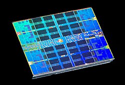
A die shot or die photography is a photo or recording of the layout of an integrated circuit, showings its design with any packaging removed. A die shot can be compared with the cross-section of an (almost) two-dimensional computer chip, on which the design and construction of various tracks and components can be clearly seen. Due to the high complexity of modern computer chips, die-shots are often displayed colourfully, with various parts coloured using special lighting or even manually.

Contents

Methods

A die shot is a picture of a computer chip without its housing. There are two ways to capture such a chip "naked" on a photo; by either taking the photo before a chip is packaged or by removing its package. [1]

Avoiding the package

Taking a photo before the chip ends up in a housing is typically preserved to the chip manufacturer, because the chip is packed fairly quickly in the production process to protect the sensitive very small parts against external influences. However, manufacturers may be reluctant to share die shots to prevent competitors from easily gaining insight into the technological progress and complexity of a chip. [2]

Removing the package

Removing the housing from a chip is typically a chemical process called decapping - a chip is so small and the parts are so microscopic that opening a housing (also named delidding) with tools such as saws, sanders or dremels could damage the chip in such a way that a die shot is no longer or less useful. [3] For example, sulphuric acid can be used to dissolve the plastic housing of a chip. Chips are immersed in a glass jar with sulphuric acid, after which the sulphuric acid is boiled for up to 45 minutes at a temperature of 337 degrees Celsius. Once the plastic housing has decayed, there may be other processes to remove leftover carbon, such as with a hot bath of concentrated nitric acid. After this, the contents of a chip are relatively exposed and a picture can be made of the chip with macrophotography or microphotography.

See also

Related Research Articles

<span class="mw-page-title-main">AMD</span> American multinational semiconductor company

Advanced Micro Devices, Inc. (AMD) is an American multinational corporation and semiconductor company based in Santa Clara, California, that develops computer processors and related technologies for business and consumer markets.

<span class="mw-page-title-main">Pin grid array</span> Type of integrated circuit packaging with the pins mounted on the underside of the package

A pin grid array (PGA) is a type of integrated circuit packaging. In a PGA, the package is square or rectangular, and the pins are arranged in a regular array on the underside of the package. The pins are commonly spaced 2.54 mm (0.1") apart, and may or may not cover the entire underside of the package.

<span class="mw-page-title-main">Mobile processor</span>

A mobile processor is a microprocessor designed for mobile devices such as laptops, and cell phones.

<span class="mw-page-title-main">Land grid array</span> Type of surface-mount packaging for integrated circuits

The land grid array (LGA) is a type of surface-mount packaging for integrated circuits (ICs) that is notable for having the pins on the socket — as opposed to pins on the integrated circuit, known as a pin grid array (PGA). An LGA can be electrically connected to a printed circuit board (PCB) either by the use of a socket or by soldering directly to the board.

<span class="mw-page-title-main">Multi-chip module</span> Electronic assembly containing multiple integrated circuits that behaves as a unit

A multi-chip module (MCM) is generically an electronic assembly where multiple integrated circuits, semiconductor dies and/or other discrete components are integrated, usually onto a unifying substrate, so that in use it can be treated as if it were a larger IC. Other terms for MCM packaging include "heterogeneous integration" or "hybrid integrated circuit". The advantage of using MCM packaging is it allows a manufacturer to use multiple components for modularity and/or to improve yields over a conventional monolithic IC approach.

<span class="mw-page-title-main">AMD APU</span> Series of microprocessors by AMD

AMD Accelerated Processing Unit (APU), formerly known as Fusion, is a series of 64-bit microprocessors from Advanced Micro Devices (AMD), combining a general-purpose AMD64 central processing unit (CPU) and 3D integrated graphics processing unit (IGPU) on a single die.

The FMA instruction set is an extension to the 128 and 256-bit Streaming SIMD Extensions instructions in the x86 microprocessor instruction set to perform fused multiply–add (FMA) operations. There are two variants:

<span class="mw-page-title-main">AMD FX</span> Series of high-end microprocessors by AMD

AMD FX is a series of high-end AMD microprocessors for personal computers which debuted in 2011, claimed as AMD's first native 8-core desktop processor. The line was introduced with the Bulldozer microarchitecture at launch, and was then succeeded by its derivative Piledriver in 2012.

Zen is the codename for a family of computer processor microarchitectures from AMD, first launched in February 2017 with the first generation of its Ryzen CPUs. It is used in Ryzen, Ryzen Threadripper, and Epyc (server).

<span class="mw-page-title-main">Zen (first generation)</span> 2017 AMD 14-nanometre processor microarchitecture

Zen is the codename for the first iteration in a family of computer processor microarchitectures of the same name from AMD. It was first used with their Ryzen series of CPUs in February 2017. The first Zen-based preview system was demonstrated at E3 2016, and first substantially detailed at an event hosted a block away from the Intel Developer Forum 2016. The first Zen-based CPUs, codenamed "Summit Ridge", reached the market in early March 2017, Zen-derived Epyc server processors launched in June 2017 and Zen-based APUs arrived in November 2017.

<span class="mw-page-title-main">Socket AM4</span> CPU socket for AMD processors with Zen and Excavator architectures

Socket AM4 is a PGA microprocessor socket used by AMD's central processing units (CPUs) built on the Zen and Excavator microarchitectures.

<span class="mw-page-title-main">Zen 2</span> 2019 AMD 7-nanometre processor microarchitecture

Zen 2 is a computer processor microarchitecture by AMD. It is the successor of AMD's Zen and Zen+ microarchitectures, and is fabricated on the 7 nm MOSFET node from TSMC. The microarchitecture powers the third generation of Ryzen processors, known as Ryzen 3000 for the mainstream desktop chips, Ryzen 4000U/H and Ryzen 5000U for mobile applications, as Threadripper 3000 for high-end desktop systems, and as Ryzen 4000G for accelerated processing units (APUs). The Ryzen 3000 series CPUs were released on 7 July 2019, while the Zen 2-based Epyc server CPUs were released on 7 August 2019. An additional chip, the Ryzen 9 3950X, was released in November 2019.

Decapping (decapsulation) or delidding of an integrated circuit is the process of removing the protective cover or integrated heat spreader (IHS) of an integrated circuit so that the contained die is revealed for visual inspection of the micro circuitry imprinted on the die. This process is typically done in order to debug a manufacturing problem with the chip, or possibly to copy information from the device, to check for counterfeit chips or to reverse engineer it. Companies such as TechInsights and ChipRebel decap, take die shots of, and reverse engineer chips for customers. Modern integrated circuits can be encapsulated in plastic, ceramic, or epoxy packages.

<span class="mw-page-title-main">Ryzen</span> AMD brand for microprocessors

Ryzen is a brand of multi-core x86-64 microprocessors designed and marketed by Advanced Micro Devices (AMD) for desktop, mobile, server, and embedded platforms based on the Zen microarchitecture. It consists of central processing units (CPUs) marketed for mainstream, enthusiast, server, and workstation segments and accelerated processing units (APUs) marketed for mainstream and entry-level segments and embedded systems applications.

Transient execution CPU vulnerabilities are vulnerabilities in a computer system in which a speculative execution optimization implemented in a microprocessor is exploited to leak secret data to an unauthorized party. The archetype is Spectre, and transient execution attacks like Spectre belong to the cache-attack category, one of several categories of side-channel attacks. Since January 2018 many different cache-attack vulnerabilities have been identified.

<span class="mw-page-title-main">Zen 4</span> 2022 AMD 5-nanometer processor microarchitecture

Zen 4 is the codename for a CPU microarchitecture designed by AMD, released on September 27, 2022. It is the successor to Zen 3 and uses TSMC's N6 process for I/O dies, N5 process for CCDs, and N4 process for APUs. Zen 4 powers Ryzen 7000 performance desktop processors, Ryzen 8000G series mainstream desktop APUs, and Ryzen Threadripper 7000 series HEDT and workstation processors. It is also used in extreme mobile processors, thin & light mobile processors, as well as EPYC 8004/9004 server processors.

<span class="mw-page-title-main">Socket AM5</span> CPU socket for AMD Ryzen processors with Zen architecture

Socket AM5 is a zero insertion force flip-chip land grid array (LGA) CPU socket designed by Advanced Micro Devices (AMD) that is used for AMD Ryzen microprocessors starting with the Zen 4 microarchitecture. AM5 was launched in September 2022 and is the successor to AM4.

References

  1. Anthony, Sebastian (2012-11-21). "How to crack open some computer chips and take your own die shots - ExtremeTech". www.extremetech.com. Archived from the original on 2022-02-27. Retrieved 2022-02-27.
  2. List, Jenny (2017-06-02). "Die Shot | Hackaday". Hackaday. Archived from the original on 2022-02-28. Retrieved 2022-02-28.
  3. Messiah, Metal (2020-11-10). "AMD Ryzen 5000 Zen 3 'Vermeer' CPU die shot pictured, revealing the core topology and architecture". DSOGaming. Archived from the original on 2022-02-28. Retrieved 2022-02-28.