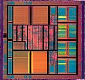
Die (integrated circuit)

Last updated
LM2576T monolithic integrated circuit die LM2576T Damaged die.jpg
LM2576T monolithic integrated circuit die

A die, in the context of integrated circuits, is a small block of semiconducting material on which a given functional circuit is fabricated. Typically, integrated circuits are produced in large batches on a single wafer of electronic-grade silicon (EGS) or other semiconductor (such as GaAs) through processes such as photolithography. The wafer is cut (diced) into many pieces, each containing one copy of the circuit. Each of these pieces is called a die.

Contents

1-watt red power LED die 1 watt red power led.jpg
1-watt red power LED die

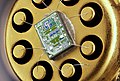
There are three commonly used plural forms: dice, dies, and die. [1] [2] To simplify handling and integration onto a printed circuit board, most dies are packaged in various forms.

Manufacturing process

Most dies are composed of silicon and used for integrated circuits. The process begins with the production of monocrystalline silicon ingots. These ingots are then sliced into disks with a diameter of up to 300 mm. [3] [4]

Typical NPN transistor. Size of die is roughly 1 mm x 1 mm. Typical NPN Transistor.jpg
Typical NPN transistor. Size of die is roughly 1 mm × 1 mm.

These wafers are then polished to a mirror finish before going through photolithography. In many steps the transistors are manufactured and connected with metal interconnect layers. These prepared wafers then go through wafer testing to test their functionality. The wafers are then sliced and sorted to filter out the faulty dies. Functional dies are then packaged and the completed integrated circuit is ready to be shipped.

Uses

A die can host many types of circuits. One common use case of an integrated circuit die is in the form of a Central Processing Unit (CPU). Through advances in modern technology, the size of the transistor within the die has shrunk exponentially, following Moore's Law. Other uses for dies can range from LED lighting to power semiconductor devices.

Images

See also

Related Research Articles

<span class="mw-page-title-main">Integrated circuit</span> Electronic circuit formed on a small, flat piece of semiconductor material

An integrated circuit, also known as a microchip or IC, is a small electronic device made up of multiple interconnected electronic components such as transistors, resistors, and capacitors. These components are etched onto a small piece of semiconductor material, usually silicon. Integrated circuits are used in a wide range of electronic devices, including computers, smartphones, and televisions, to perform various functions such as processing and storing information. They have greatly impacted the field of electronics by enabling device miniaturization and enhanced functionality.

<span class="mw-page-title-main">Semiconductor device fabrication</span> Manufacturing process used to create integrated circuits

Semiconductor device fabrication is the process used to manufacture semiconductor devices, typically integrated circuits (ICs) such as computer processors, microcontrollers, and memory chips that are present in everyday electronic devices. It is a multiple-step photolithographic and physio-chemical process during which electronic circuits are gradually created on a wafer, typically made of pure single-crystal semiconducting material. Silicon is almost always used, but various compound semiconductors are used for specialized applications.

<span class="mw-page-title-main">Very Large Scale Integration</span> Creating an integrated circuit by combining many transistors into a single chip

Very-large-scale integration (VLSI) is the process of creating an integrated circuit (IC) by combining millions or billions of MOS transistors onto a single chip. VLSI began in the 1970s when MOS integrated circuit chips were developed and then widely adopted, enabling complex semiconductor and telecommunication technologies. The microprocessor and memory chips are VLSI devices.

<span class="mw-page-title-main">Semiconductor device</span> Electronic component that exploits the electronic properties of semiconductor materials

A semiconductor device is an electronic component that relies on the electronic properties of a semiconductor material for its function. Its conductivity lies between conductors and insulators. Semiconductor devices have replaced vacuum tubes in most applications. They conduct electric current in the solid state, rather than as free electrons across a vacuum or as free electrons and ions through an ionized gas.

<span class="mw-page-title-main">Flip chip</span> Technique that flips a microchip upside down to connect it

Flip chip, also known as controlled collapse chip connection or its abbreviation, C4, is a method for interconnecting dies such as semiconductor devices, IC chips, integrated passive devices and microelectromechanical systems (MEMS), to external circuitry with solder bumps that have been deposited onto the chip pads. The technique was developed by General Electric's Light Military Electronics Department, Utica, New York. The solder bumps are deposited on the chip pads on the top side of the wafer during the final wafer processing step. In order to mount the chip to external circuitry, it is flipped over so that its top side faces down, and aligned so that its pads align with matching pads on the external circuit, and then the solder is reflowed to complete the interconnect. This is in contrast to wire bonding, in which the chip is mounted upright and fine wires are welded onto the chip pads and lead frame contacts to interconnect the chip pads to external circuitry.

<span class="mw-page-title-main">Integrated circuit packaging</span> Final stage of semiconductor device fabrication

Integrated circuit packaging is the final stage of semiconductor device fabrication, in which the die is encapsulated in a supporting case that prevents physical damage and corrosion. The case, known as a "package", supports the electrical contacts which connect the device to a circuit board.

<span class="mw-page-title-main">Planar process</span> Process used to make microchips

The planar process is a manufacturing process used in the semiconductor industry to build individual components of a transistor, and in turn, connect those transistors together. It is the primary process by which silicon integrated circuit chips are built, and it is the most commonly used method of producing junctions during the manufacture of semiconductor devices. The process utilizes the surface passivation and thermal oxidation methods.

<span class="mw-page-title-main">Stepper</span> Photolithographic Tool

A stepper is a device used in the manufacture of integrated circuits (ICs). It is an essential part of the process of photolithography, which creates millions of microscopic circuit elements on the surface of silicon wafers out of which chips are made. It is similar in operation to a slide projector or a photographic enlarger. The ICs that are made form the heart of computer processors, memory chips, and many other electronic devices.

<span class="mw-page-title-main">System in a package</span> Electronic component

A system in a package (SiP) or system-in-package is a number of integrated circuits (ICs) enclosed in one chip carrier package or encompassing an IC package substrate that may include passive components and perform the functions of an entire system. The ICs may be stacked using package on package, placed side by side, and/or embedded in the substrate. The SiP performs all or most of the functions of an electronic system, and is typically used when designing components for mobile phones, digital music players, etc. Dies containing integrated circuits may be stacked vertically on the package substrate. They are internally connected by fine wires that are bonded to the package substrate. Alternatively, with a flip chip technology, solder bumps are used to join stacked chips together and to the package substrate, or even both techniques can be used in a single package. SiPs are like systems on a chip (SoCs) but less tightly integrated and not on a single semiconductor die.

Die singulation, also called wafer dicing, is the process in semiconductor device fabrication by which dies are separated from a finished wafer of semiconductor. Die singulation comes after the photolithography process. It can involve scribing and breaking, mechanical sawing or laser cutting. All methods are typically automated to ensure precision and accuracy. Following the dicing process the individual silicon chips may be encapsulated into chip carriers which are then suitable for use in building electronic devices such as computers, etc.

In semiconductor electronics fabrication technology, a self-aligned gate is a transistor manufacturing approach whereby the gate electrode of a MOSFET is used as a mask for the doping of the source and drain regions. This technique ensures that the gate is naturally and precisely aligned to the edges of the source and drain.

The term die shrink refers to the scaling of metal–oxide–semiconductor (MOS) devices. The act of shrinking a die creates a somewhat identical circuit using a more advanced fabrication process, usually involving an advance of lithographic nodes. This reduces overall costs for a chip company, as the absence of major architectural changes to the processor lowers research and development costs while at the same time allowing more processor dies to be manufactured on the same piece of silicon wafer, resulting in less cost per product sold.

<span class="mw-page-title-main">Through-silicon via</span> Metal-plated holes used to vertically and electrically connect several dies that are atop each other

In electronic engineering, a through-silicon via (TSV) or through-chip via is a vertical electrical connection (via) that passes completely through a silicon wafer or die. TSVs are high-performance interconnect techniques used as an alternative to wire-bond and flip chips to create 3D packages and 3D integrated circuits. Compared to alternatives such as package-on-package, the interconnect and device density is substantially higher, and the length of the connections becomes shorter.

A three-dimensional integrated circuit is a MOS integrated circuit (IC) manufactured by stacking as many as 16 or more ICs and interconnecting them vertically using, for instance, through-silicon vias (TSVs) or Cu-Cu connections, so that they behave as a single device to achieve performance improvements at reduced power and smaller footprint than conventional two dimensional processes. The 3D IC is one of several 3D integration schemes that exploit the z-direction to achieve electrical performance benefits in microelectronics and nanoelectronics.

Monocrystalline silicon, more often called single-crystal silicon, in short mono c-Si or mono-Si, is the base material for silicon-based discrete components and integrated circuits used in virtually all modern electronic equipment. Mono-Si also serves as a photovoltaic, light-absorbing material in the manufacture of solar cells.

<span class="mw-page-title-main">Beam lead technology</span> Technology used to deposit metal beams onto integrated circuits for connecting them

Beam lead technology is a method of fabricating a semiconductor device. Its initial application was for high-frequency silicon switching transistors and high-speed integrated circuits. This technology eliminated the labor-intensive wire-bonding process that was commonly used for integrated circuits at the time. It also enabled the automated assembly of semiconductor chips onto larger substrates, facilitating the production of hybrid integrated circuits.

<span class="mw-page-title-main">Integrated passive devices</span>

Integrated passive devices (IPDs), also known as integrated passive components (IPCs) or embedded passive components (EPC), are electronic components where resistors (R), capacitors (C), inductors (L)/coils/chokes, microstriplines, impedance matching elements, baluns or any combinations of them are integrated in the same package or on the same substrate. Sometimes integrated passives can also be called as embedded passives, and still the difference between integrated and embedded passives is technically unclear. In both cases passives are realized in between dielectric layers or on the same substrate.

<span class="mw-page-title-main">Wafer-level packaging</span> Means of packaging an integrated circuit

Wafer-level packaging (WLP) is a process where packaging components are attached to an integrated circuit (IC) before the wafer – on which the IC is fabricated – is diced. In WSP, the top and bottom layers of the packaging and the solder bumps are attached to the integrated circuits while they are still in the wafer. This process differs from a conventional process, in which the wafer is sliced into individual circuits (dice) before the packaging components are attached.

A semiconductor package is a metal, plastic, glass, or ceramic casing containing one or more discrete semiconductor devices or integrated circuits. Individual components are fabricated on semiconductor wafers before being diced into die, tested, and packaged. The package provides a means for connecting it to the external environment, such as printed circuit board, via leads such as lands, balls, or pins; and protection against threats such as mechanical impact, chemical contamination, and light exposure. Additionally, it helps dissipate heat produced by the device, with or without the aid of a heat spreader. There are thousands of package types in use. Some are defined by international, national, or industry standards, while others are particular to an individual manufacturer.

Glossary of microelectronics manufacturing terms

References

  1. John E. Ayers (2004). Digital Integrated Circuits. CRC Press. ISBN   0-8493-1951-X. Archived from the original on 2017-01-31.
  2. Robert Allen Meyers (2000). Encyclopedia of Physical Science and Technology. Academic Press. ISBN   0-12-226930-6.
  3. From Sand to Silicon “Making of a Chip” | Intel. (YouTube video, streamed on Nov 6, 2009)
  4. From Sand to Silicon “Making of a Chip” Illustrations. (n.d.)