Technique used to connect a microchip to its package
Gold wire ball-bonded on a silicon dieAluminium wires wedge-bonded to a BC160 transistor dieThe interconnections in a power package are made using thick (250 to 400 μm), wedge-bonded, aluminium wires.Inside a wire-bonded BGA package. This package has an Nvidia GeForce 256 GPU.
Wire bonding is a method of making interconnections between an integrated circuit (IC) or other semiconductor device and its packaging during semiconductor device fabrication. Wire bonding can also be used to connect an IC to other electronics or to connect from one printed circuit board (PCB) to another, although these are less common. Wire bonding is generally considered the most cost-effective and flexible interconnect technology and is used to assemble the vast majority of semiconductor packages. Wire bonding can be used at frequencies above 100GHz.[1]
Wire diameters start from under 10 μm and can be up to several hundred micrometres for high-powered applications.
The wire bonding industry is transitioning from gold to copper.[2][3][4] This change has been instigated by the rising cost of gold and the comparatively stable, and much lower, cost of copper. While possessing higher thermal and electrical conductivity than gold, copper had previously been seen as less reliable due to its hardness and susceptibility to corrosion. By 2015, it is expected that more than a third of all wire bonding machines in use will be set up for copper.[5]
Copper wire has become one of the preferred materials for wire bonding interconnects in many semiconductor and microelectronic applications. Copper is used for fine wire ball bonding in sizes from 10 micrometers (0.00039in) up to 75 micrometers (0.003in).[6] Copper wire has the ability of being used at smaller diameters providing the same performance as gold without the high material cost. Smaller diameters are possible due to copper's higher electrical conductivity. Copper wire bonds are at least as reliable if not more reliable than gold wire bonds.[7]
Copper wire up to 500 micrometers (0.02in)[8] can be successfully wedge bonded. Large diameter copper wire can and does replace aluminium wire where high current carrying capacity is needed or where there are problems with complex geometry. Annealing and process steps used by manufacturers enhance the ability to use large diameter copper wire to wedge bond to silicon without damage occurring to the die.
Copper wire does pose some challenges in that it is harder than both gold and aluminium, so bonding parameters must be kept under tight control. The amount of power used during ultrasonic bonding must be higher[9] and copper has a higher fusing current so it has a higher current carrying capacity.[10] The formation of oxides is inherent with this material, so storage and shelf life are issues that must be considered.[7] Special packaging is required in order to protect copper wire and achieve a longer shelf life. Palladium coated copper wire is a common alternative which has shown significant resistance to corrosion, albeit at a higher hardness than pure copper and a greater price, though still less than gold. During the fabrication of wire bonds, copper wire, as well as its plated varieties, must be worked in the presence of forming gas [95% nitrogen and 5% hydrogen] or a similar anoxic gas in order to prevent corrosion. A method for coping with copper's relative hardness is the use of high purity [5N+] varieties.[5]
Long-term corrosion effects (Cu2Si) and other stability topics led to increased quality requirements when used in automotive applications.[11]
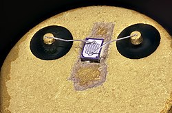
Red–green–blue surface mount LED package with gold wire bonding details
Pure gold wire doped with controlled amounts of beryllium and other elements is normally used for ball bonding. This process brings together the two materials that are to be bonded using heat, pressure and ultrasonic energy referred to as thermosonic bonding. The most common approach in thermosonic bonding is to ball-bond to the chip, then stitch-bond to the substrate. Very tight controls during processing enhance looping characteristics and eliminate sagging.
Junction size, bond strength and conductivity requirements typically determine the most suitable wire size for a specific wire bonding application. Typical manufacturers make gold wire in diameters from 8 micrometers (0.00031in) and larger. Production tolerance on gold wire diameter is +/-3%.
Alloyed aluminium wires are generally preferred to pure aluminium wire except in high-current devices because of greater drawing ease to fine sizes and higher pull-test strengths in finished devices. Pure aluminium and 0.5% magnesium-aluminium are most commonly used in sizes larger than 100 micrometers (0.0039in).
All-aluminium systems in semiconductor fabrication eliminate the "purple plague" (brittle gold-aluminium intermetallic compound) sometimes associated with pure gold bonding wire. Aluminium is particularly suitable for thermosonic bonding.
In order to assure that high quality bonds can be obtained at high production speeds, special controls are used in the manufacture of 1% silicon-aluminium wire. One of the most important characteristics of high grade bonding wire of this type is homogeneity of the alloy system. Homogeneity is given special attention during the manufacturing process. Microscopic checks of the alloy structure of finished lots of 1% silicon-aluminium wire are performed routinely. Processing also is carried out under conditions which yield the ultimate in surface cleanliness and smooth finish and permits entirely snag-free de-reeling.
Attachment techniques
Demonstration of ultrasonic wedge bonding of an aluminium wire between gold electrodes on a printed circuit board and gold electrodes on a sapphire substrate, reverse bonding order
Ball bonding usually is restricted to gold and copper wire and usually requires heat. For wedge bonding, only gold wire requires heat. Wedge bonding can use large diameter wires or wire ribbons for power electronics application. Ball bonding is limited to small diameter wires, suitable for interconnect application.
In either type of wire bonding, the wire is attached at both ends using a combination of downward pressure, ultrasonic energy, and in some cases heat, to make a weld. Heat is used to make the metal softer. The correct combination of temperature and ultrasonic energy is used in order to maximize the reliability and strength of a wire bond. If heat and ultrasonic energy is used, the process is called thermosonic bonding.
In wedge bonding, the wire must be drawn in a straight line according to the first bond. This slows down the process due to time needed for tool alignment. Ball bonding, however, creates its first bond in a ball shape with the wire sticking out at the top, having no directional preference. Thus, the wire can be drawn in any direction, making it a faster process.
Compliant bonding[12] transmits heat and pressure through a compliant or indentable aluminium tape and therefore is applicable in bonding gold wires and the beam leads that have been electroformed to the silicon integrated circuit (known as the beam leaded integrated circuit).
Manufacturing and reliability challenges
There are multiple challenges when it comes to wire bond manufacturing and reliability. These challenges tend of be a function of several parameters such as the material systems, bonding parameters, and use environment. Different wire bond-bond pad metal systems such as Aluminium-Aluminium (Al-Al), Gold-Aluminium (Au-Al), and Copper-Aluminium (Cu-Al) require different manufacturing parameters and behave differently under the same use environments.
Wire bond manufacturing
Much work has been done to characterize various metal systems, review critical manufacturing parameters, and identify typical reliability issues that occur in wire bonding.[13][14] When it comes to material selection, the application and use environment will dictate the metal system. Often the electrical properties, mechanical properties, and cost are taken into account when making a decision. For example, a high current device for a space application might require a large diameter aluminium wire bond in a hermetically sealed ceramic package. If cost is a large constraint, then avoiding gold wire bonds may be a necessity. Some recent work has been done to look at copper wire bonds in automotive applications.[15] This is only a small sampling, as there is a vast body of work reviewing and testing what material systems work best in different applications.
From a manufacturing perspective, the bonding parameters play a critical role in bond formation and bond quality. Parameters such bond force, ultrasonic energy, temperature, and loop geometry, to name a few, can have a significant effect on bond quality. There are various wire bonding techniques (thermosonic bonding, ultrasonic bonding, thermocompression bonding) and types of wire bonds (ball bonding, wedge bonding) that affect susceptibility to manufacturing defects and reliability issues. Certain materials and wire diameters are more practical for fine pitch or complex layouts. The bond pad also plays an important role as the metallization and barrier layer(s) stackup will impact the bond formation.
Typical failure modes that result from poor bond quality and manufacturing defects include: fracture at the ball bond neck, heel cracking (wedge bonds), pad liftoff, pad peel, overcompression, and improper intermetallic formation. A combination of wire bond pull/shear testing, nondestructive testing, and destructive physical analysis (DPA) can be used to screen manufacturing and quality issues.
Wire bond reliability
While wirebond manufacturing tends to focus on bond quality, it often does not account for wearout mechanisms related to wire bond reliability. In this case, an understanding of the application and use environment can help prevent reliability issues. Common examples of environments that lead to wire bond failures include elevated temperature, humidity, and temperature cycling.[16]
Under elevated temperatures, excessive intermetallics (IMC) growth can create brittle points of fracture. Much work that has been done to characterize the intermetallic formation and aging for various metal systems. This not a problem in metal systems where the wire bond and bond pad are the same material such as Al-Al. This does become a concern in dissimilar metal systems. One of the most well known examples is the brittle intermetallics formed in gold-aluminium IMCs such as purple plague. Additionally, diffusion related issues, such as Kirkendall voiding and Horsting voiding, can also lead to wire bond failures.
Under elevated temperature and humidity environments, corrosion can be a concern. This is most common in Au-Al metal systems and is driven by galvanic corrosion. The presence of halides such as chlorine can accelerate this behavior. This Au-Al corrosion is often characterized with Peck's law for temperature and humidity. This is not as common in other metal systems.
Under temperature cycling, thermomechanical stress is generated in the wire bond as a result of coefficient of thermal expansion (CTE) mismatch between the epoxy molding compound (EMC), the leadframe, the die, the die adhesive, and the wire bond. This leads to low cycle fatigue due to shear or tensile stresses in the wire bond. Various fatigue models have been used to predict the fatigue life of wire bonds under such conditions, such as Paris' law.[17] Fatigue models can be coupled with data-driven approaches, such as physics-informed Markov-Chains,[18] to account for uncertainty and to better generalize for predictions on lower temperature.
Proper understanding of the use environment and metal systems are often the most important factors for increasing wire bond reliability.
Testing
While there are some wire bond pull and shear testing techniques such as MIL-STD-883, ASTM F459-13, and JESD22-B116,[19][20][21][22] these tend to be applicable for manufacturing quality rather than reliability. They are often monotonic overstress techniques, where peak force and fracture location are the critical outputs. In this case the damage is plasticity dominated, and does not reflect some wearout mechanisms that might be seen under environmental conditions.
Wire pull testing applies an upward force under the wire, effectively pulling it away from the substrate or die.[23] The purpose of the test is as MIL-STD-883 2011.9 describes it: "To measure bond strengths, evaluate bond strength distributions, or determine compliance with specified bond strength requirements". A wire can be pulled to destruction, but there are also non-destructive variants whereby one tests whether the wire can withstand a certain force. Non-destructive test methods are typically used for 100% testing of safety critical, high quality and high cost products, avoiding damage to the acceptable wired bonds tested.
The term wire pull usually refers to the act of pulling a wire with a hook mounted on a pull sensor on a bond tester. However, to promote certain failure modes, wires can be cut and then pulled by tweezers, also mounted on a pull sensor on a bond tester. Usually wires up to 75μm diameter (3 mil) are classified as thin wire. Beyond that size, we speak about thick wire testing.
↑Ghrabli, Mehdi; Bouarroudj, Mounira; Chamoin, Ludovic; Aldea, Emanuel (2024). Hybrid modeling for remaining useful life prediction in power module prognosis. 2024 25th International Conference on Thermal Mechanical and Multi-Physics Simulation and Experiments in Microelectronics and Microsystems (EuroSimE). Catania, Italy: IEEE. doi:10.1109/EuroSimE60745.2024.10491493.
This page is based on this Wikipedia article Text is available under the CC BY-SA 4.0 license; additional terms may apply. Images, videos and audio are available under their respective licenses.