Morton B. Panish

Last updated
Morton Panish
Born (1929-04-08) April 8, 1929 (age 95)
Brooklyn, New York
CitizenshipAmerican
Alma mater Michigan State University
Known for Semiconductor lasers
SpouseEvelyn Wally Chaim (20 August 1951) [1]
ChildrenSteven Chaim Panish, Paul William Panish, Deborah Faye Panish [1]
Awards C&C Prize, IEEE Morris N. Liebmann Memorial Award; member of the National Academy of Sciences and National Academy of Engineering [2]
Scientific career
Fields Physical chemistry
Institutions Oak Ridge National Laboratory, Avco, Bell Labs [2]
Thesis  (1954)
Doctoral advisor Max Rogers [3]

Morton B. Panish (born April 8, 1929) is an American physical chemist who, with Izuo Hayashi, developed a room-temperature continuous wave semiconductor laser in 1970. For this achievement he shared the Kyoto Prize in Advanced Technology in 2001.

Contents

Panish was elected to the National Academy of Engineering in 1986 and to the National Academy of Sciences in 1987.

Biography

Early life and education

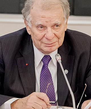
Morton Panish was born in Brooklyn on April 8, 1929 to Isidore Panish and Fanny Panish (née Glasser) and grew up in Brooklyn. [1] [2] At the age of 12, he was strongly influenced by a book called Microbe Hunters by Paul de Kruif, which left him with the impression that a scientific career is exciting. He went to Erasmus Hall High School, where he was fascinated by a chemistry substitute teacher's description of his Ph.D. work at Columbia University, which involved synthesizing new organic compounds. He graduated in 1947, attended Brooklyn College for two years and then transferred to the University of Denver. He graduated in 1950. He met his future wife, Evelyn Chaim, in a chemistry class shortly after arriving in Denver. They married during his first year in graduate school.

Panish enrolled in graduate school at Michigan State University, majoring in physical chemistry and minoring in organic chemistry. His master's thesis involved a "series of measurements of the electric dipole behavior of some organic compounds," and he did not consider it very challenging. [3] His advisor was Max Rogers, a Canadian and former student of Linus Pauling, and Rogers supervised his Ph.D. work as well, which was on interhalogen compounds. Used to process reactor fuels, these compounds are highly reactive and dangerous, and after Panish had completed his experiments, another student was badly injured in an explosion. He resolved to work with less dangerous materials in future. [3]

Career

From 1954 to 1957 Panish worked for Oak Ridge National Laboratory in Tennessee, studying the chemical thermodynamics of molten salts, then he moved to Massachusetts and worked in the Research and Advanced Development Division of AVCO Corporation. The primary contract of this division, with the United States Air Force, was to develop vehicles for the reentry of thermonuclear weapons into the atmosphere. Panish was unwilling to do this work, but the government allotted 5% of the budget to basic research. From 1957 to 1964 he worked on the chemical thermodynamics of refractory compounds, but then decided to leave because the government terminated the funding for basic research. [2] [3]

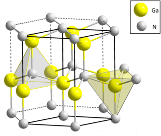
Before the Oak Ridge job, Panish had applied to Bell Labs and been rejected, but now they hired him. He started work in June 1964 in the Solid State Electronics Research Laboratory, a group headed by physicist John Galt. He was part of a department working on III-V semiconductors, compounds in which elements from group III and group V of the periodic table are combined, for example, gallium arsenide (GaAs). He planned a series of experiments to determine the phase diagrams among solid solutions of the various III-V compounds and to look into controlling the impurity elements that determine the electrical properties of those semiconductors. [3]

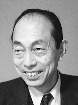
In 1966, Galt asked Panish and Izuo Hayashi, a physicist from Japan, to investigate a problem involving laser diodes. The first such lasers, also known as injection lasers, were developed independently in 1962 by General Electric groups in Syracuse and Schenectady as well as the Thomas J. Watson Research Center of IBM and the MIT Lincoln Laboratory. [4] These early lasers, mostly made out of a single chunk of GaAs, required high current densities to operate, so they could only run continuously at very low temperatures; at room temperature, they could only operate for a fraction of a second. For them to be used in a practical communications system, they would need to operate continuously at room temperature. [3]

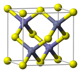
A solution to the problem was proposed theoretically by Herbert Kroemer in 1963 a double heterojunction laser but Kroemer failed to suggest that a suitable (lattice matched) combination of III-V semiconductors would be needed to provide ideal interfaces between the III-V compounds with their different bandgaps. The combination of such materials used for the first CW lasers was GaAs (Gallium Arsenide) and Aluminum Gallium Arsenide, which have the same lattice parameter. The idea was to place a material like GaAs, with a smaller band gap, between two layers of a material such as aluminum gallium arsenide (a solid solution of AlAs and GaAs) that had a larger band gap; this confined the charge carriers and the optical field (the light) to this layer, reducing the current needed for lasing. [5] :151 Panish and Izuo Hayashi independently developed the single heterostructure laser first and then the double heterostructure laser. However, publication of the announcement of the first room temperature continuously operating double heterostructure laser was by Zhores Alferov in 1970 one month before Hayashi and Panish published similar results. Although there was some degree of contact between the group in Leningrad and the group in New Jersey including a visit by Alferov to the New Jersey lab, and a visit by Panish and Hayashi to Alferov’s lab in Leningrad, the two achievements were obtained independently. Panish experimented with making wafers using a new form of liquid-phase epitaxy while Hayashi tested the laser properties. Panish and Hayashi observed what they thought might be CW operation in several wafers in the weeks before their final demonstration. That had to await a laser that lived long enough for a complete plot of the lasing spectrum to be achieved. Over the Memorial Day weekend in 1970, while Panish was at home, Hayashi tried a diode and it emitted a continuous-wave beam with just over 24 degrees Celsius and he was able to plot the complete spectrum with the very slow equipment available at the time.

Room-temperature lasers were soon duplicated at RCA Laboratories, Standard Telecommunication Laboratories and Nippon Electric Corporation (NEC). Over the next few years, the lasers became longer-lasting and more reliable. At Bell Labs, the job of creating a practical device was given to Barney DeLoach. But in January 1973, they told him to cease all work on the problem. As he recalled, their view was "We've already got air, we've already got copper. Who needs a new medium?" [5] :157

The continuous wave semiconductor laser led directly to the light sources in fiber-optic communication, laser printers, barcode readers and optical disc drives, but it was mostly Japanese entrepreneurs, not AT&T, that ended up profiting from these technologies. [6] :252 [7] The Japanese success was enhanced by Panish’s ex-partner Izuo Hayashi who had returned to Japan.

After the work on double heterostructure lasers Panish continued to demonstrate variants of the laser structures with other collaborators in work done through the late 1970s, but the major thrust of his work for the rest of his career, until 1992, was to exploit the new opportunities presented by the use of Molecular Beam Epitaxy to produce lattice matched semiconductor heterostructures in III-V systems other than GaAs-AlGaAs for other devices (detectors, quantum well physics and devices, ultra fast hererostructure transistors) and for the study of the physics of small layered structures.

Awards and honors

Works

The following are some of the major works by Panish: [2]

Related Research Articles

<span class="mw-page-title-main">Zhores Alferov</span> Soviet-Russian physicist (1930–2019)

Zhores Ivanovich Alferov was a Soviet and Russian physicist and academic who contributed significantly to the creation of modern heterostructure physics and electronics. He shared the 2000 Nobel Prize in Physics for the development of the semiconductor heterojunction for optoelectronics. He also became a politician in his later life, serving in the lower house of the Russian parliament, the State Duma, as a member of the Communist Party from 1995.

<span class="mw-page-title-main">Aluminium gallium arsenide</span> Semiconductor material

Aluminium gallium arsenide (AlxGa1−xAs) is a semiconductor material with very nearly the same lattice constant as GaAs, but a larger bandgap. The x in the formula above is a number between 0 and 1 - this indicates an arbitrary alloy between GaAs and AlAs.

<span class="mw-page-title-main">Laser diode</span> Semiconductor laser

A laser diode is a semiconductor device similar to a light-emitting diode in which a diode pumped directly with electrical current can create lasing conditions at the diode's junction.

<span class="mw-page-title-main">Gallium arsenide</span> Chemical compound

Gallium arsenide (GaAs) is a III-V direct band gap semiconductor with a zinc blende crystal structure.

<span class="mw-page-title-main">Gallium nitride</span> Chemical compound

Gallium nitride is a binary III/V direct bandgap semiconductor commonly used in blue light-emitting diodes since the 1990s. The compound is a very hard material that has a Wurtzite crystal structure. Its wide band gap of 3.4 eV affords it special properties for applications in optoelectronic, high-power and high-frequency devices. For example, GaN is the substrate that makes violet (405 nm) laser diodes possible, without requiring nonlinear optical frequency doubling.

<span class="mw-page-title-main">Blue laser</span> Laser which emits light with blue wavelengths

A blue laser emits electromagnetic radiation with a wavelength between 400 and 500 nanometers, which the human eye sees in the visible spectrum as blue or violet.

Indium gallium arsenide (InGaAs) is a ternary alloy of indium arsenide (InAs) and gallium arsenide (GaAs). Indium and gallium are group III elements of the periodic table while arsenic is a group V element. Alloys made of these chemical groups are referred to as "III-V" compounds. InGaAs has properties intermediate between those of GaAs and InAs. InGaAs is a room-temperature semiconductor with applications in electronics and photonics.

<span class="mw-page-title-main">Indium arsenide</span> Chemical compound

Indium arsenide, InAs, or indium monoarsenide, is a narrow-bandgap semiconductor composed of indium and arsenic. It has the appearance of grey cubic crystals with a melting point of 942 °C.

Aluminium gallium indium phosphide is a semiconductor material that provides a platform for the development of multi-junction photovoltaics and optoelectronic devices. It has a direct bandgap ranging from ultraviolet to infrared photon energies.

Gallium arsenide phosphide is a semiconductor material, an alloy of gallium arsenide and gallium phosphide. It exists in various composition ratios indicated in its formula by the fraction x.

<span class="mw-page-title-main">Gallium antimonide</span> Chemical compound

Gallium antimonide (GaSb) is a semiconducting compound of gallium and antimony of the III-V family. It has a room temperature lattice constant of about 0.610 nm. It has a room temperature direct bandgap of approximately 0.73 eV.

<span class="mw-page-title-main">Isamu Akasaki</span> Japanese engineer (1929–2021)

Isamu Akasaki was a Japanese engineer and physicist, specializing in the field of semiconductor technology and Nobel Prize laureate, best known for inventing the bright gallium nitride (GaN) p-n junction blue LED in 1989 and subsequently the high-brightness GaN blue LED as well.

<span class="mw-page-title-main">Dmitri Z. Garbuzov</span> Russian-born American inventor

Dmitri Z. Garbuzov was one of the pioneers and inventors of room temperature continuous-wave-operating diode lasers and high-power diode lasers.

Milton Feng co-created the first transistor laser, working with Nick Holonyak in 2004. The paper discussing their work was voted in 2006 as one of the five most important papers published by the American Institute of Physics since its founding 75 years ago. In addition to the invention of transistor laser, he is also well known for inventions of other "major breakthrough" devices, including the world's fastest transistor and light-emitting transistor (LET). As of May, 2009 he is a professor at the University of Illinois at Urbana–Champaign and holds the Nick Holonyak Jr. Endowed Chair Professorship.

<span class="mw-page-title-main">Izuo Hayashi</span> Japanese physicist

Izuo Hayashi was a Japanese physicist.

A quantum-well laser is a laser diode in which the active region of the device is so narrow that quantum confinement occurs. Laser diodes are formed in compound semiconductor materials that are able to emit light efficiently. The wavelength of the light emitted by a quantum-well laser is determined by the width of the active region rather than just the bandgap of the materials from which it is constructed. This means that much shorter wavelengths can be obtained from quantum-well lasers than from conventional laser diodes using a particular semiconductor material. The efficiency of a quantum-well laser is also greater than a conventional laser diode due to the stepwise form of its density of states function.

James J. Coleman is an electrical engineer who worked at Bell Labs, Rockwell International, and the University of Illinois, Urbana. He is best known for his work on semiconductor lasers, materials and devices including strained-layer indium gallium arsenide lasers and selective area epitaxy. Coleman is a Fellow of the IEEE and a member of the US National Academy of Engineering.

<span class="mw-page-title-main">Rubin Braunstein</span> American physicist and educator (1922–2018)

Rubin Braunstein (1922–2018) was an American physicist and educator. In 1955 he published the first measurements of light emission by semiconductor diodes made from crystals of gallium arsenide (GaAs), gallium antimonide (GaSb), and indium phosphide (InP). GaAs, GaSb, and InP are examples of III-V semiconductors. The III-V semiconductors absorb and emit light much more strongly than silicon, which is the best-known semiconductor. Braunstein's devices are the forerunners of contemporary LED lighting and semiconductor lasers, which typically employ III-V semiconductors. The 2000 and 2014 Nobel Prizes in Physics were awarded for further advances in closely related fields.

Thulium phosphide is an inorganic compound of thulium and phosphorus with the chemical formula TmP.

Aluminium gallium antimonide, also known as gallium aluminium antimonide or AlGaSb (AlxGa1-xSb), is a ternary III-V semiconductor compound. It can be considered as an alloy between aluminium antimonide and gallium antimonide. The alloy can contain any ratio between aluminium and gallium. AlGaSb refers generally to any composition of the alloy.

References

  1. 1 2 3 Panish, Morton. "Morton Panish (b. April 08, 1929)". The Families of Mort and Evelyn Panish. Ancestry.com. Retrieved 7 April 2014.
  2. 1 2 3 4 5 "Morton B. Panish: Profile". Kyoto Prize. Inamori Foundation. Archived from the original on 9 April 2014. Retrieved 7 April 2014.
  3. 1 2 3 4 5 6 "Morton B. Panish: Commemorative lecture" (PDF). Kyoto Prize. Inamori Foundation. Archived from the original (PDF) on 17 April 2014. Retrieved 7 April 2014.
  4. Coleman, J J (1 September 2012). "The development of the semiconductor laser diode after the first demonstration in 1962". Semiconductor Science and Technology. 27 (9): 090207. Bibcode:2012SeScT..27i0207C. doi:10.1088/0268-1242/27/9/090207. S2CID   95751174.
  5. 1 2 Hecht, Jeff (2004). City of light : the story of fiber optics (Rev. and expanded ed.). Oxford [u.a.]: Oxford Univ. Press. pp. 152–157. ISBN   9780195162554.
  6. Johnstone, Bob (2000). We were burning : Japanese entrepreneurs and the forging of the electronic age. New York: BasicBooks. ISBN   9780465091188.
  7. "Morton B. Panish: CItation". Kyoto Prize. Inamori Foundation. Archived from the original on 8 April 2014. Retrieved 7 April 2014.