
Transmission electron microscopy (TEM) is a microscopy technique in which a beam of electrons is transmitted through a specimen to form an image. The specimen is most often an ultrathin section less than 100 nm thick or a suspension on a grid. An image is formed from the interaction of the electrons with the sample as the beam is transmitted through the specimen. The image is then magnified and focused onto an imaging device, such as a fluorescent screen, a layer of photographic film, or a detector such as a scintillator attached to a charge-coupled device or a direct electron detector.
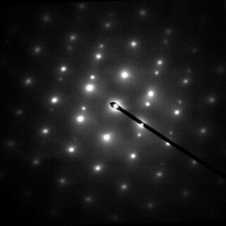
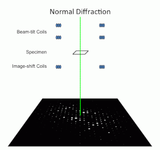
Electron diffraction is a generic term for phenomena associated with changes in the direction of electron beams due to elastic interactions with atoms. It occurs due to elastic scattering, when there is no change in the energy of the electrons. The negatively charged electrons are scattered due to Coulomb forces when they interact with both the positively charged atomic core and the negatively charged electrons around the atoms. The resulting map of the directions of the electrons far from the sample is called a diffraction pattern, see for instance Figure 1. Beyond patterns showing the directions of electrons, electron diffraction also plays a major role in the contrast of images in electron microscopes.
Electron backscatter diffraction (EBSD) is a scanning electron microscopy (SEM) technique used to study the crystallographic structure of materials. EBSD is carried out in a scanning electron microscope equipped with an EBSD detector comprising at least a phosphorescent screen, a compact lens and a low-light camera. In the microscope an incident beam of electrons hits a tilted sample. As backscattered electrons leave the sample, they interact with the atoms and are both elastically diffracted and lose energy, leaving the sample at various scattering angles before reaching the phosphor screen forming Kikuchi patterns (EBSPs). The EBSD spatial resolution depends on many factors, including the nature of the material under study and the sample preparation. They can be indexed to provide information about the material's grain structure, grain orientation, and phase at the micro-scale. EBSD is used for impurities and defect studies, plastic deformation, and statistical analysis for average misorientation, grain size, and crystallographic texture. EBSD can also be combined with energy-dispersive X-ray spectroscopy (EDS), cathodoluminescence (CL), and wavelength-dispersive X-ray spectroscopy (WDS) for advanced phase identification and materials discovery.
Electron crystallography is a method to determine the arrangement of atoms in solids using a transmission electron microscope (TEM). It can involve the use of high-resolution transmission electron microscopy images, electron diffraction patterns including convergent-beam electron diffraction or combinations of these. It has been successful in determining some bulk structures, and also surface structures. Two related methods are low-energy electron diffraction which has solved the structure of many surfaces, and reflection high-energy electron diffraction which is used to monitor surfaces often during growth.

A scanning transmission electron microscope (STEM) is a type of transmission electron microscope (TEM). Pronunciation is [stɛm] or [ɛsti:i:ɛm]. As with a conventional transmission electron microscope (CTEM), images are formed by electrons passing through a sufficiently thin specimen. However, unlike CTEM, in STEM the electron beam is focused to a fine spot which is then scanned over the sample in a raster illumination system constructed so that the sample is illuminated at each point with the beam parallel to the optical axis. The rastering of the beam across the sample makes STEM suitable for analytical techniques such as Z-contrast annular dark-field imaging, and spectroscopic mapping by energy dispersive X-ray (EDX) spectroscopy, or electron energy loss spectroscopy (EELS). These signals can be obtained simultaneously, allowing direct correlation of images and spectroscopic data.
Electron holography is holography with electron matter waves. It was invented by Dennis Gabor in 1948 when he tried to improve image resolution in electron microscope. The first attempts to perform holography with electron waves were made by Haine and Mulvey in 1952; they recorded holograms of zinc oxide crystals with 60 keV electrons, demonstrating reconstructions with approximately 1 nm resolution. In 1955, G. Möllenstedt and H. Düker invented an electron biprism, thus enabling the recording of electron holograms in off-axis scheme. There are many different possible configurations for electron holography, with more than 20 documented in 1992 by Cowley. Usually, high spatial and temporal coherence of the electron beam are required to perform holographic measurements.

John Maxwell Cowley was an American Regents Professor at Arizona State University. The John M. Cowley Center for High-Resolution Electron Microscopy at Arizona State is named in his honor.
John Cowley was an extraordinarily productive scientist over more than five decades. He made pioneering contributions in the fields of electron microscopy, diffraction and crystallography, all of which brought him widespread recognition. He received the highest awards of the International Union of Crystallography, the Electron Microscopy Society of America and the American Crystallographic Society, and he was honored by election to Fellowship of the Australian Academy of Science, The Royal Society of London, and the American Physical Society. His monograph Diffraction Physics remains the standard reference in the field. His ideas, enthusiasm and basic understanding of electron optics and diffraction phenomena provided a valued source of leadership to many generations of students and co-workers, and he was universally admired by his peers and colleagues as a great and inspiring scientist.

Electron tomography (ET) is a tomography technique for obtaining detailed 3D structures of sub-cellular, macro-molecular, or materials specimens. Electron tomography is an extension of traditional transmission electron microscopy and uses a transmission electron microscope to collect the data. In the process, a beam of electrons is passed through the sample at incremental degrees of rotation around the center of the target sample. This information is collected and used to assemble a three-dimensional image of the target. For biological applications, the typical resolution of ET systems are in the 5–20 nm range, suitable for examining supra-molecular multi-protein structures, although not the secondary and tertiary structure of an individual protein or polypeptide. Recently, atomic resolution in 3D electron tomography reconstructions has been demonstrated.

Rafal Edward Dunin-Borkowski HonFRMS is a British experimental physicist. He is currently Director of the Institute for Microstructure Research (PGI-5) and the Ernst Ruska-Centre for Microscopy and Spectroscopy with Electrons (ER-C) in Forschungszentrum Jülich and Professor of Experimental Physics in RWTH Aachen University.

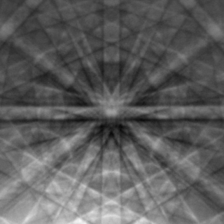
Ptychography is a computational method of microscopic imaging. It generates images by processing many coherent interference patterns that have been scattered from an object of interest. Its defining characteristic is translational invariance, which means that the interference patterns are generated by one constant function moving laterally by a known amount with respect to another constant function. The interference patterns occur some distance away from these two components, so that the scattered waves spread out and "fold" into one another as shown in the figure.

Crystallographic image processing (CIP) is traditionally understood as being a set of key steps in the determination of the atomic structure of crystalline matter from high-resolution electron microscopy (HREM) images obtained in a transmission electron microscope (TEM) that is run in the parallel illumination mode. The term was created in the research group of Sven Hovmöller at Stockholm University during the early 1980s and became rapidly a label for the "3D crystal structure from 2D transmission/projection images" approach. Since the late 1990s, analogous and complementary image processing techniques that are directed towards the achieving of goals with are either complementary or entirely beyond the scope of the original inception of CIP have been developed independently by members of the computational symmetry/geometry, scanning transmission electron microscopy, scanning probe microscopy communities, and applied crystallography communities.
Henning Sirringhaus is Hitachi Professor of Electron Device Physics, Head of the Microelectronics Group and a member of the Optoelectronics Group at the Cavendish Laboratory. He is also a Fellow of Churchill College at the University of Cambridge.
Precession electron diffraction (PED) is a specialized method to collect electron diffraction patterns in a transmission electron microscope (TEM). By rotating (precessing) a tilted incident electron beam around the central axis of the microscope, a PED pattern is formed by integration over a collection of diffraction conditions. This produces a quasi-kinematical diffraction pattern that is more suitable as input into direct methods algorithms to determine the crystal structure of the sample.

Thomas Benjamin Britton is a materials scientist and engineer based at The University of British Columbia. He is a specialist in micromechanics, electron microscopy and crystal plasticity. In 2014 he was awarded the Silver Medal of the Institute of Materials, Minerals and Mining (IOM3), a society of which he then became a Fellow in 2016.
John Marius Rodenburg is emeritus professor in the Department of Electronic and Electrical Engineering at the University of Sheffield. He was elected a Fellow of the Royal Society (FRS) in 2019 for "internationally recognised... work on revolutionising the imaging capability of light, X-ray and electron transmission microscopes".
Peter David Nellist, is a British physicist and materials scientist, currently a professor in the Department of Materials at the University of Oxford. He is noted for pioneering new techniques in high-resolution electron microscopy.
4D scanning transmission electron microscopy is a subset of scanning transmission electron microscopy (STEM) which utilizes a pixelated electron detector to capture a convergent beam electron diffraction (CBED) pattern at each scan location. This technique captures a 2 dimensional reciprocal space image associated with each scan point as the beam rasters across a 2 dimensional region in real space, hence the name 4D STEM. Its development was enabled by evolution in STEM detectors and improvements computational power. The technique has applications in visual diffraction imaging, phase orientation and strain mapping, phase contrast analysis, among others.
Angus J Wilkinson is a professor of materials science based at University of Oxford. He is a specialist in micromechanics, electron microscopy and crystal plasticity. He assists in overseeing the MicroMechanics group while focusing on the fundamentals of material deformation. He developed the HR-EBSD method for mapping stress and dislocation density at high spatial resolution used at the micron scale in mechanical testing and micro-cantilevers to extract data on mechanical properties that are relevant to materials engineering.
Angus Ian KirklandFInstP FRSC FRMS is the JEOL Professor of Electron Microscopy at the Department of Materials, University of Oxford. Professor Kirkland specialises in High-resolution transmission electron microscopy and Scanning transmission electron microscopy.

Transmission Kikuchi Diffraction (TKD), also sometimes called transmission-electron backscatter diffraction (t-EBSD), is a method for orientation mapping at the nanoscale. It’s used for analysing the microstructures of thin transmission electron microscopy (TEM) specimens in the scanning electron microscope (SEM). This technique has been widely utilised in the characterization of nano-crystalline materials, including oxides, superconductors, and metallic alloys.
