Related Research Articles

A scanning electron microscope (SEM) is a type of electron microscope that produces images of a sample by scanning the surface with a focused beam of electrons. The electrons interact with atoms in the sample, producing various signals that contain information about the surface topography and composition of the sample. The electron beam is scanned in a raster scan pattern, and the position of the beam is combined with the intensity of the detected signal to produce an image. In the most common SEM mode, secondary electrons emitted by atoms excited by the electron beam are detected using a secondary electron detector. The number of secondary electrons that can be detected, and thus the signal intensity, depends, among other things, on specimen topography. Some SEMs can achieve resolutions better than 1 nanometer.

X-ray fluorescence (XRF) is the emission of characteristic "secondary" X-rays from a material that has been excited by being bombarded with high-energy X-rays or gamma rays. The phenomenon is widely used for elemental analysis and chemical analysis, particularly in the investigation of metals, glass, ceramics and building materials, and for research in geochemistry, forensic science, archaeology and art objects such as paintings.
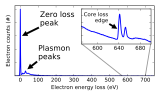
Electron energy loss spectroscopy (EELS) is a form of electron microscopy in which a material is exposed to a beam of electrons with a known, narrow range of kinetic energies. Some of the electrons will undergo inelastic scattering, which means that they lose energy and have their paths slightly and randomly deflected. The amount of energy loss can be measured via an electron spectrometer and interpreted in terms of what caused the energy loss. Inelastic interactions include phonon excitations, inter- and intra-band transitions, plasmon excitations, inner shell ionizations, and Cherenkov radiation. The inner-shell ionizations are particularly useful for detecting the elemental components of a material. For example, one might find that a larger-than-expected number of electrons comes through the material with 285 eV less energy than they had when they entered the material. This is approximately the amount of energy needed to remove an inner-shell electron from a carbon atom, which can be taken as evidence that there is a significant amount of carbon present in the sample. With some care, and looking at a wide range of energy losses, one can determine the types of atoms, and the numbers of atoms of each type, being struck by the beam. The scattering angle can also be measured, giving information about the dispersion relation of whatever material excitation caused the inelastic scattering.

Transmission electron microscopy (TEM) is a microscopy technique in which a beam of electrons is transmitted through a specimen to form an image. The specimen is most often an ultrathin section less than 100 nm thick or a suspension on a grid. An image is formed from the interaction of the electrons with the sample as the beam is transmitted through the specimen. The image is then magnified and focused onto an imaging device, such as a fluorescent screen, a layer of photographic film, or a detector such as a scintillator attached to a charge-coupled device or a direct electron detector.
Particle-induced X-ray emission or proton-induced X-ray emission (PIXE) is a technique used for determining the elemental composition of a material or a sample. When a material is exposed to an ion beam, atomic interactions occur that give off EM radiation of wavelengths in the x-ray part of the electromagnetic spectrum specific to an element. PIXE is a powerful yet non-destructive elemental analysis technique now used routinely by geologists, archaeologists, art conservators and others to help answer questions of provenance, dating and authenticity.

A synchrotron light source is a source of electromagnetic radiation (EM) usually produced by a storage ring, for scientific and technical purposes. First observed in synchrotrons, synchrotron light is now produced by storage rings and other specialized particle accelerators, typically accelerating electrons. Once the high-energy electron beam has been generated, it is directed into auxiliary components such as bending magnets and insertion devices in storage rings and free electron lasers. These supply the strong magnetic fields perpendicular to the beam that are needed to stimulate the high energy electrons to emit photons.
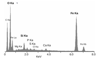
Energy-dispersive X-ray spectroscopy, sometimes called energy dispersive X-ray analysis or energy dispersive X-ray microanalysis (EDXMA), is an analytical technique used for the elemental analysis or chemical characterization of a sample. It relies on an interaction of some source of X-ray excitation and a sample. Its characterization capabilities are due in large part to the fundamental principle that each element has a unique atomic structure allowing a unique set of peaks on its electromagnetic emission spectrum. The peak positions are predicted by the Moseley's law with accuracy much better than experimental resolution of a typical EDX instrument.

X-ray spectroscopy is a general term for several spectroscopic techniques for characterization of materials by using x-ray radiation.

An electron microprobe (EMP), also known as an electron probe microanalyzer (EPMA) or electron micro probe analyzer (EMPA), is an analytical tool used to non-destructively determine the chemical composition of small volumes of solid materials. It works similarly to a scanning electron microscope: the sample is bombarded with an electron beam, emitting x-rays at wavelengths characteristic to the elements being analyzed. This enables the abundances of elements present within small sample volumes to be determined, when a conventional accelerating voltage of 15-20 kV is used. The concentrations of elements from lithium to plutonium may be measured at levels as low as 100 parts per million (ppm), material dependent, although with care, levels below 10 ppm are possible. The ability to quantify lithium by EPMA became a reality in 2008.

A scanning transmission electron microscope (STEM) is a type of transmission electron microscope (TEM). Pronunciation is [stɛm] or [ɛsti:i:ɛm]. As with a conventional transmission electron microscope (CTEM), images are formed by electrons passing through a sufficiently thin specimen. However, unlike CTEM, in STEM the electron beam is focused to a fine spot which is then scanned over the sample in a raster illumination system constructed so that the sample is illuminated at each point with the beam parallel to the optical axis. The rastering of the beam across the sample makes STEM suitable for analytical techniques such as Z-contrast annular dark-field imaging, and spectroscopic mapping by energy dispersive X-ray (EDX) spectroscopy, or electron energy loss spectroscopy (EELS). These signals can be obtained simultaneously, allowing direct correlation of images and spectroscopic data.
High resolution electron energy loss spectroscopy (HREELS) is a tool used in surface science. The inelastic scattering of electrons from surfaces is utilized to study electronic excitations or vibrational modes of the surface of a material or of molecules adsorbed to a surface. In contrast to other electron energy loss spectroscopies (EELS), HREELS deals with small energy losses in the range of 10−3 eV to 1 eV. It plays an important role in the investigation of surface structure, catalysis, dispersion of surface phonons and the monitoring of epitaxial growth.

Focused ion beam, also known as FIB, is a technique used particularly in the semiconductor industry, materials science and increasingly in the biological field for site-specific analysis, deposition, and ablation of materials. A FIB setup is a scientific instrument that resembles a scanning electron microscope (SEM). However, while the SEM uses a focused beam of electrons to image the sample in the chamber, a FIB setup uses a focused beam of ions instead. FIB can also be incorporated in a system with both electron and ion beam columns, allowing the same feature to be investigated using either of the beams. FIB should not be confused with using a beam of focused ions for direct write lithography. These are generally quite different systems where the material is modified by other mechanisms.

The hard X-ray nanoprobe at the Center for Nanoscale Materials (CNM), Argonne National Lab advanced the state of the art by providing a hard X-ray microscopy beamline with the highest spatial resolution in the world. It provides for fluorescence, diffraction, and transmission imaging with hard X-rays at a spatial resolution of 30 nm or better. A dedicated source, beamline, and optics form the basis for these capabilities. This unique instrument is not only key to the specific research areas of the CNM; it will also be a general utility, available to the broader nanoscience community in studying nanomaterials and nanostructures, particularly for embedded structures.
Annular dark-field imaging is a method of mapping samples in a scanning transmission electron microscope (STEM). These images are formed by collecting scattered electrons with an annular dark-field detector.

Dark-field microscopy describes microscopy methods, in both light and electron microscopy, which exclude the unscattered beam from the image. Consequently, the field around the specimen is generally dark.
Richard D. Leapman is an English physicist who is current scientific director of National Institute of Biomedical Imaging and Bioengineering (NIBIB), since October 2006 and a chief of the laboratory of bioengineering and physical science. Leapman's research interests are in the development and application of quantitative electron microscopy and the application of novel nanoscale imaging methods to solve problems in structural and cellular biology.
Scanning transmission X-ray microscopy (STXM) is a type of X-ray microscopy in which a zone plate focuses an X-ray beam onto a small spot, a sample is scanned in the focal plane of the zone plate and the transmitted X-ray intensity is recorded as a function of the sample position. A stroboscopic scheme is used where the excitation is the pump and the synchrotron X-ray flashes are the probe. X-ray microscopes work by exposing a film or charged coupled device detector to detect X-rays that pass through the specimen. The image formed is of a thin section of specimen. Newer X-ray microscopes use X-ray absorption spectroscopy to heterogeneous materials at high spatial resolution. The essence of the technique is a combination of spectromicroscopy, imaging with spectral sensitivity, and microspectroscopy, recording spectra from very small spots.

The scanning helium microscope (SHeM) is a novel form of microscopy that uses low-energy (5–100 meV) neutral helium atoms to image the surface of a sample without any damage to the sample caused by the imaging process. Since helium is inert and neutral, it can be used to study delicate and insulating surfaces. Images are formed by rastering a sample underneath an atom beam and monitoring the flux of atoms that are scattered into a detector at each point.
Photon-Induced Near-field Electron Microscopy (PINEM) is a variant of the Ultrafast Transmission Electron Microscopy technique and is based on the inelastic coupling between electrons and photons in presence of a surface or a nanostructure. This method allows one to investigate time-varying nanoscale electromagnetic fields in an electron microscope.