Electron energy loss spectroscopy

Last updated
Experimental electron energy loss spectrum, showing the major features: zero-loss peak, plasmon peaks and core loss edge. Electron energy loss spectrum feature overview.svg
Experimental electron energy loss spectrum, showing the major features: zero-loss peak, plasmon peaks and core loss edge.

Electron energy loss spectroscopy (EELS) is a form of electron microscopy in which a material is exposed to a beam of electrons with a known, narrow range of kinetic energies. Some of the electrons will undergo inelastic scattering, which means that they lose energy and have their paths slightly and randomly deflected. The amount of energy loss can be measured via an electron spectrometer and interpreted in terms of what caused the energy loss. Inelastic interactions include phonon excitations, inter- and intra-band transitions, plasmon excitations, inner shell ionizations, and Cherenkov radiation. The inner-shell ionizations are particularly useful for detecting the elemental components of a material. For example, one might find that a larger-than-expected number of electrons comes through the material with 285  eV less energy than they had when they entered the material. This is approximately the amount of energy needed to remove an inner-shell electron from a carbon atom, which can be taken as evidence that there is a significant amount of carbon present in the sample. With some care, and looking at a wide range of energy losses, one can determine the types of atoms, and the numbers of atoms of each type, being struck by the beam. The scattering angle (that is, the amount that the electron's path is deflected) can also be measured, giving information about the dispersion relation of whatever material excitation caused the inelastic scattering. [1]

Contents

History

The technique was developed by James Hillier and RF Baker in the mid-1940s [2] but was not widely used over the next 50 years, only becoming more widespread in research in the 1990s due to advances in microscope instrumentation and vacuum technology. With modern instrumentation becoming widely available in laboratories worldwide, the technical and scientific developments from the mid-1990s have been rapid. The technique is able to take advantage of modern aberration-corrected probe forming systems to attain spatial resolutions down to ~0.1 nm, while with a monochromated electron source and/or careful deconvolution the energy resolution can be 0.1 eV or better. [3] This has enabled detailed measurements of the atomic and electronic properties of single columns of atoms, and in a few cases, of single atoms. [4] [5]

Comparison with EDX

EELS is spoken of as being complementary to energy-dispersive x-ray spectroscopy (variously called EDX, EDS, XEDS, etc.), which is another common spectroscopy technique available on many electron microscopes. EDX excels at identifying the atomic composition of a material, is quite easy to use, and is particularly sensitive to heavier elements. EELS has historically been a more difficult technique but is in principle capable of measuring atomic composition, chemical bonding, valence and conduction band electronic properties, surface properties, and element-specific pair distance distribution functions. [6] EELS tends to work best at relatively low atomic numbers, where the excitation edges tend to be sharp, well-defined, and at experimentally accessible energy losses (the signal being very weak beyond about 3 keV energy loss). EELS is perhaps best developed for the elements ranging from carbon through the 3d transition metals (from scandium to zinc). [7] For carbon, an experienced spectroscopist can tell at a glance the differences between diamond, graphite, amorphous carbon, and "mineral" carbon (such as the carbon appearing in carbonates). The spectra of 3d transition metals can be analyzed to identify the oxidation states of the atoms. [8] Cu(I), for instance, has a different so-called "white-line" intensity ratio than Cu(II) does. This ability to "fingerprint" different forms of the same element is a strong advantage of EELS over EDX. The difference is mainly due to the difference in energy resolution between the two techniques (~1 eV or better for EELS, perhaps a few tens of eV for EDX).

Variants

Example of inner shell ionization edge (core loss) EELS data from La0.7Sr0.3MnO3, acquired on a scanning transmission electron microscope. Electron energy loss spectroscopy coreloss lsmo.svg
Example of inner shell ionization edge (core loss) EELS data from La0.7Sr0.3MnO3, acquired on a scanning transmission electron microscope.

There are several basic flavors of EELS, primarily classified by the geometry and by the kinetic energy of the incident electrons (typically measured in kiloelectron-volts, or keV). Probably the most common today is transmission EELS, in which the kinetic energies are typically 100 to 300 keV and the incident electrons pass entirely through the material sample. Usually this occurs in a transmission electron microscope (TEM), although some dedicated systems exist which enable extreme resolution in terms of energy and momentum transfer at the expense of spatial resolution.[ citation needed ]

Other flavors include reflection EELS (including reflection high-energy electron energy-loss spectroscopy (RHEELS)), typically at 10 to 30 keV, and aloof EELS (sometimes called near-field EELS), in which the electron beam does not in fact strike the sample but instead interacts with it via the long-ranged Coulomb interaction. Aloof EELS is particularly sensitive to surface properties but is limited to very small energy losses such as those associated with surface plasmons or direct interband transitions.[ citation needed ]

Within transmission EELS, the technique is further subdivided into valence EELS (which measures plasmons and interband transitions) and inner-shell ionization EELS (which provides much the same information as x-ray absorption spectroscopy, but from much smaller volumes of material). The dividing line between the two, while somewhat ill-defined, is in the vicinity of 50 eV energy loss.

Instrumental developments have opened up the ultra-low energy loss part of the EELS spectrum, enabling vibrational spectroscopy in the TEM. [9] Both IR-active and non-IR-active vibrational modes are present in EELS. [10]

EEL spectrum

The electron energy loss (EEL) spectrum can be roughly split into two different regions: the low-loss spectrum (up until about 50eV in energy loss) and the high-loss spectrum. The low-loss spectrum contains the zero-loss peak as well as the plasmon peaks, and contains information about the band structure and dielectric properties of the sample. The high-loss spectrum contains the ionisation edges that arise due to inner shell ionisations in the sample. These are characteristic to the species present in the sample, and as such can be used to obtain accurate information about the chemistry of a sample. [11]

Thickness measurements

EELS allows quick and reliable measurement of local thickness in transmission electron microscopy. [6] The most efficient procedure is the following: [12]

The spatial resolution of this procedure is limited by the plasmon localization and is about 1 nm, [6] meaning that spatial thickness maps can be measured in scanning transmission electron microscopy with ~1 nm resolution.

Pressure measurements

The intensity and position of low-energy EELS peaks are affected by pressure. This fact allows mapping local pressure with ~1 nm spatial resolution.

Use in confocal geometry

Scanning confocal electron energy loss microscopy (SCEELM) is a new analytical microscopy tool that enables a double corrected transmission electron microscope to achieve sub-10 nm depth resolution in depth sectioning imaging of nanomaterials. [16] It was previously termed as energy filtered scanning confocal electron microscopy due to the lack to full spectrum acquisition capability (only a small energy window on the order of 5 eV can be used at a time). SCEELM takes advantages of the newly developed chromatic aberration corrector which allows electrons of more than 100 eV of energy spread to be focused to roughly the same focal plane. It has been demonstrated that a simultaneous acquisition of the zero loss, low-loss, and core loss signals up to 400 eV in the confocal geometry with depth discrimination capability.[ citation needed ]

See also

Related Research Articles

<span class="mw-page-title-main">Infrared spectroscopy</span> Measurement of infrared radiations interaction with matter

Infrared spectroscopy is the measurement of the interaction of infrared radiation with matter by absorption, emission, or reflection. It is used to study and identify chemical substances or functional groups in solid, liquid, or gaseous forms. It can be used to characterize new materials or identify and verify known and unknown samples. The method or technique of infrared spectroscopy is conducted with an instrument called an infrared spectrometer which produces an infrared spectrum. An IR spectrum can be visualized in a graph of infrared light absorbance on the vertical axis vs. frequency, wavenumber or wavelength on the horizontal axis. Typical units of wavenumber used in IR spectra are reciprocal centimeters, with the symbol cm−1. Units of IR wavelength are commonly given in micrometers, symbol μm, which are related to the wavenumber in a reciprocal way. A common laboratory instrument that uses this technique is a Fourier transform infrared (FTIR) spectrometer. Two-dimensional IR is also possible as discussed below.

<span class="mw-page-title-main">Spectroscopy</span> Study involving matter and electromagnetic radiation

Spectroscopy is the field of study that measures and interprets electromagnetic spectra. In narrower contexts, spectroscopy is the precise study of color as generalized from visible light to all bands of the electromagnetic spectrum.

<span class="mw-page-title-main">Auger electron spectroscopy</span> Analytical technique used specifically in the study of surfaces

Auger electron spectroscopy is a common analytical technique used specifically in the study of surfaces and, more generally, in the area of materials science. It is a form of electron spectroscopy that relies on the Auger effect, based on the analysis of energetic electrons emitted from an excited atom after a series of internal relaxation events. The Auger effect was discovered independently by both Lise Meitner and Pierre Auger in the 1920s. Though the discovery was made by Meitner and initially reported in the journal Zeitschrift für Physik in 1922, Auger is credited with the discovery in most of the scientific community. Until the early 1950s Auger transitions were considered nuisance effects by spectroscopists, not containing much relevant material information, but studied so as to explain anomalies in X-ray spectroscopy data. Since 1953 however, AES has become a practical and straightforward characterization technique for probing chemical and compositional surface environments and has found applications in metallurgy, gas-phase chemistry, and throughout the microelectronics industry.

<span class="mw-page-title-main">Cathodoluminescence</span> Photon emission under the impact of an electron beam

Cathodoluminescence is an optical and electromagnetic phenomenon in which electrons impacting on a luminescent material such as a phosphor, cause the emission of photons which may have wavelengths in the visible spectrum. A familiar example is the generation of light by an electron beam scanning the phosphor-coated inner surface of the screen of a television that uses a cathode ray tube. Cathodoluminescence is the inverse of the photoelectric effect, in which electron emission is induced by irradiation with photons.

<span class="mw-page-title-main">Surface science</span> Study of physical and chemical phenomena that occur at the interface of two phases

Surface science is the study of physical and chemical phenomena that occur at the interface of two phases, including solid–liquid interfaces, solid–gas interfaces, solid–vacuum interfaces, and liquid–gas interfaces. It includes the fields of surface chemistry and surface physics. Some related practical applications are classed as surface engineering. The science encompasses concepts such as heterogeneous catalysis, semiconductor device fabrication, fuel cells, self-assembled monolayers, and adhesives. Surface science is closely related to interface and colloid science. Interfacial chemistry and physics are common subjects for both. The methods are different. In addition, interface and colloid science studies macroscopic phenomena that occur in heterogeneous systems due to peculiarities of interfaces.

<span class="mw-page-title-main">Raman spectroscopy</span> Spectroscopic technique

Raman spectroscopy is a spectroscopic technique typically used to determine vibrational modes of molecules, although rotational and other low-frequency modes of systems may also be observed. Raman spectroscopy is commonly used in chemistry to provide a structural fingerprint by which molecules can be identified.

<span class="mw-page-title-main">Energy-dispersive X-ray spectroscopy</span> Analytical technique used for the elemental analysis or chemical characterization of a sample

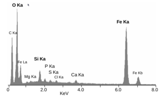
Energy-dispersive X-ray spectroscopy, sometimes called energy dispersive X-ray analysis or energy dispersive X-ray microanalysis (EDXMA), is an analytical technique used for the elemental analysis or chemical characterization of a sample. It relies on an interaction of some source of X-ray excitation and a sample. Its characterization capabilities are due in large part to the fundamental principle that each element has a unique atomic structure allowing a unique set of peaks on its electromagnetic emission spectrum. The peak positions are predicted by the Moseley's law with accuracy much better than experimental resolution of a typical EDX instrument.

<span class="mw-page-title-main">Scanning transmission electron microscopy</span> Scanning microscopy using thin samples and transmitted electrons

A scanning transmission electron microscope (STEM) is a type of transmission electron microscope (TEM). Pronunciation is [stɛm] or [ɛsti:i:ɛm]. As with a conventional transmission electron microscope (CTEM), images are formed by electrons passing through a sufficiently thin specimen. However, unlike CTEM, in STEM the electron beam is focused to a fine spot which is then scanned over the sample in a raster illumination system constructed so that the sample is illuminated at each point with the beam parallel to the optical axis. The rastering of the beam across the sample makes STEM suitable for analytical techniques such as Z-contrast annular dark-field imaging, and spectroscopic mapping by energy dispersive X-ray (EDX) spectroscopy, or electron energy loss spectroscopy (EELS). These signals can be obtained simultaneously, allowing direct correlation of images and spectroscopic data.

High resolution electron energy loss spectroscopy (HREELS) is a tool used in surface science. The inelastic scattering of electrons from surfaces is utilized to study electronic excitations or vibrational modes of the surface of a material or of molecules adsorbed to a surface. In contrast to other electron energy loss spectroscopies (EELS), HREELS deals with small energy losses in the range of 10−3 eV to 1 eV. It plays an important role in the investigation of surface structure, catalysis, dispersion of surface phonons and the monitoring of epitaxial growth.

<span class="mw-page-title-main">Inelastic mean free path</span> Index of how far electrons travel through a solid before losing energy

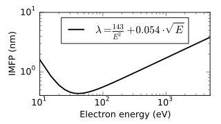
The inelastic mean free path (IMFP) is an index of how far an electron on average travels through a solid before losing energy.

Energy-filtered transmission electron microscopy (EFTEM) is a technique used in transmission electron microscopy, in which only electrons of particular kinetic energies are used to form the image or diffraction pattern. The technique can be used to aid chemical analysis of the sample in conjunction with complementary techniques such as electron crystallography.

<span class="mw-page-title-main">Characterization (materials science)</span> Study of material structure and properties

Characterization, when used in materials science, refers to the broad and general process by which a material's structure and properties are probed and measured. It is a fundamental process in the field of materials science, without which no scientific understanding of engineering materials could be ascertained. The scope of the term often differs; some definitions limit the term's use to techniques which study the microscopic structure and properties of materials, while others use the term to refer to any materials analysis process including macroscopic techniques such as mechanical testing, thermal analysis and density calculation. The scale of the structures observed in materials characterization ranges from angstroms, such as in the imaging of individual atoms and chemical bonds, up to centimeters, such as in the imaging of coarse grain structures in metals.

Inelastic electron tunneling spectroscopy (IETS) is an experimental tool for studying the vibrations of molecular adsorbates on metal oxides. It yields vibrational spectra of the adsorbates with high resolution (< 0.5 meV) and high sensitivity (< 1013 molecules are required to provide a spectrum). An additional advantage is the fact that optically forbidden transitions may be observed as well. Within IETS, an oxide layer with molecules adsorbed on it is put between two metal plates. A bias voltage is applied between the two contacts. An energy diagram of the metal-oxide-metal device under bias is shown in the top figure. The metal contacts are characterized by a constant density of states, filled up to the Fermi energy. The metals are assumed to be equal. The adsorbates are situated on the oxide material. They are represented by a single bridge electronic level, which is the upper dashed line. If the insulator is thin enough, there is a finite probability that the incident electron tunnels through the barrier. Since the energy of the electron is not changed by this process, it is an elastic process. This is shown in the left figure.

<span class="mw-page-title-main">Raman microscope</span> Laser microscope used for Raman spectroscopy

The Raman microscope is a laser-based microscopic device used to perform Raman spectroscopy. The term MOLE is used to refer to the Raman-based microprobe. The technique used is named after C. V. Raman, who discovered the scattering properties in liquids.

<span class="mw-page-title-main">Resonant inelastic X-ray scattering</span> Advanced X-ray spectroscopy technique

Resonant inelastic X-ray scattering (RIXS) is an advanced X-ray spectroscopy technique.

The technique of vibrational analysis with scanning probe microscopy allows probing vibrational properties of materials at the submicrometer scale, and even of individual molecules. This is accomplished by integrating scanning probe microscopy (SPM) and vibrational spectroscopy. This combination allows for much higher spatial resolution than can be achieved with conventional Raman/FTIR instrumentation. The technique is also nondestructive, requires non-extensive sample preparation, and provides more contrast such as intensity contrast, polarization contrast and wavelength contrast, as well as providing specific chemical information and topography images simultaneously.

<span class="mw-page-title-main">Ondrej Krivanek</span> British physicist

Ondrej L. Krivanek is a Czech/British physicist resident in the United States, and a leading developer of electron-optical instrumentation. He won the Kavli Prize for Nanoscience in 2020 for his substantial innovations in atomic resolution electron microscopy.

Electron magnetic circular dichroism (EMCD) is the EELS equivalent of XMCD.

<span class="mw-page-title-main">Brent Fultz</span> American materials scientist

Brent Fultz is an American physicist and materials scientist and one of the world's leading authorities on statistical mechanics, diffraction, and phase transitions in materials. Fultz is the Barbara and Stanley Rawn Jr. Professor of Applied Physics and Materials Science at the California Institute of Technology. He is known for his research in materials physics and materials chemistry, and for establishing the importance of phonon entropy to the phase stability of materials. Additionally, Fultz oversaw the construction of the wide angular-range chopper spectrometer (ARCS) instrument at the Spallation Neutron Source and has made advances in phonon measuring techniques.

References

  1. Egerton, R. F. (2009). "Electron energy-loss spectroscopy in the TEM". Reports on Progress in Physics. 72 (1): 016502. Bibcode:2009RPPh...72a6502E. doi:10.1088/0034-4885/72/1/016502. S2CID   120421818.
  2. Baker, J.; Hillier, R. F. (September 1944). "Microanalysis by means of electrons". J. Appl. Phys. 15 (9): 663–675. Bibcode:1944JAP....15..663H. doi:10.1063/1.1707491.
  3. Rose, H. H. (1 April 2008). "Optics of high-performance electron microscopes". Science and Technology of Advanced Materials. 9 (1): 014107. Bibcode:2008STAdM...9a4107R. doi:10.1088/0031-8949/9/1/014107. PMC   5099802 . PMID   27877933.
  4. Ramasse, Quentin M.; Seabourne, Che R.; Kepaptsoglou, Despoina-Maria; Zan, Recep; Bangert, Ursel; Scott, Andrew J. (October 2013). "Probing the Bonding and Electronic Structure of Single Atom Dopants in Graphene with Electron Energy Loss Spectroscopy". Nano Letters. 13 (10): 4989–4995. Bibcode:2013NanoL..13.4989R. doi:10.1021/nl304187e. ISSN   1530-6984. PMID   23259533. S2CID   68082.
  5. Tan, H.; Turner, S.; Yücelen, E.; Verbeeck, J.; Van Tendeloo, G. (September 2011). "2D atomic mapping of oxidation states in transition metal oxides by scanning transmission electron microscopy and electron energy-loss spectroscopy". Phys. Rev. Lett. 107 (10): 107602. Bibcode:2011PhRvL.107j7602T. doi:10.1103/PhysRevLett.107.107602. hdl: 10067/912650151162165141 . PMID   21981530.
  6. 1 2 3 Egerton 1996.
  7. Ahn C C (ed.) (2004) Transmission electron energy loss spectrometry in material science and the EELS Atlas, Wiley, Weinheim, Germany, doi : 10.1002/3527605495, ISBN   3527405658
  8. Riedl, T.; T. Gemming; W. Gruner; J. Acker; K. Wetzig (April 2007). "Determination of manganese valency in La1−xSrxMnO3 using ELNES in the (S)TEM". Micron. 38 (3): 224–230. doi:10.1016/j.micron.2006.06.017. PMID   16962785.
  9. Krivanek, Ondrej L.; Lovejoy, Tracy C.; Dellby, Niklas; Aoki, Toshihiro; Carpenter, R. W.; Rez, Peter; Soignard, Emmanuel; Zhu, Jiangtao; Batson, Philip E.; Lagos, Maureen J.; Egerton, Ray F. (2014). "Vibrational spectroscopy in the electron microscope". Nature. 514 (7521): 209–212. Bibcode:2014Natur.514..209K. doi:10.1038/nature13870. ISSN   0028-0836. PMID   25297434. S2CID   4467249.
  10. Venkatraman, Kartik; Levin, Barnaby D.A.; March, Katia; Rez, Peter; Crozier, Peter A. (2019). "Vibrational spectroscopy at atomic resolution with electron impact scattering". Nature Physics. 15 (12): 1237–1241. arXiv: 1812.08895 . doi:10.1038/s41567-019-0675-5. S2CID   119452520.
  11. Hofer, F.; et al. (2016). "Fundamentals of electron energy loss spectroscopy". IOP Conference Series: Materials Science and Engineering. 109: 012007. doi: 10.1088/1757-899X/109/1/012007 .
  12. Iakoubovskii, K.; Mitsuishi, K.; Nakayama, Y.; Furuya, K. (2008). "Thickness measurements with electron energy loss spectroscopy" (PDF). Microscopy Research and Technique. 71 (8): 626–31. CiteSeerX   10.1.1.471.3663 . doi:10.1002/jemt.20597. PMID   18454473. S2CID   24604858.
  13. Iakoubovskii, Konstantin; Mitsuishi, Kazutaka; Nakayama, Yoshiko; Furuya, Kazuo (2008). "Mean free path of inelastic electron scattering in elemental solids and oxides using transmission electron microscopy: Atomic number dependent oscillatory behavior" (PDF). Physical Review B. 77 (10): 104102. Bibcode:2008PhRvB..77j4102I. doi:10.1103/PhysRevB.77.104102.
  14. Taverna, D.; Kociak, M.; Stéphan, O.; Fabre, A.; Finot, E.; Décamps, B.; Colliex, C. (2008). "Probing Physical Properties of Confined Fluids within Individual Nanobubbles". Physical Review Letters. 100 (3): 035301. arXiv: 0704.2306 . Bibcode:2008PhRvL.100c5301T. doi:10.1103/PhysRevLett.100.035301. PMID   18232994. S2CID   4028240.
  15. Iakoubovskii, Konstantin; Mitsuishi, Kazutaka; Furuya, Kazuo (2008). "Structure and pressure inside Xe nanoparticles embedded in Al" (PDF). Physical Review B. 78 (6): 064105. Bibcode:2008PhRvB..78f4105I. doi:10.1103/PhysRevB.78.064105.
  16. Xin, Huolin L.; et al. (2013). "Scanning Confocal Electron Energy-Loss Microscopy Using Valence-Loss Signals". Microscopy and Microanalysis. 19 (4): 1036–1049. Bibcode:2013MiMic..19.1036X. doi:10.1017/S1431927613001438. PMID   23692691. S2CID   25818886.

Further reading