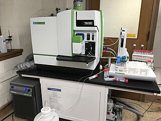
Inductively coupled plasma mass spectrometry (ICP-MS) is a type of mass spectrometry that uses an inductively coupled plasma to ionize the sample. It atomizes the sample and creates atomic and small polyatomic ions, which are then detected. It is known and used for its ability to detect metals and several non-metals in liquid samples at very low concentrations. It can detect different isotopes of the same element, which makes it a versatile tool in isotopic labeling.
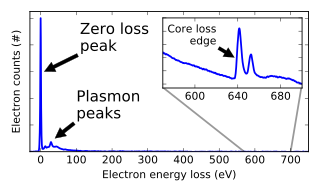
Electron energy loss spectroscopy (EELS) is a form of electron microscopy in which a material is exposed to a beam of electrons with a known, narrow range of kinetic energies. Some of the electrons will undergo inelastic scattering, which means that they lose energy and have their paths slightly and randomly deflected. The amount of energy loss can be measured via an electron spectrometer and interpreted in terms of what caused the energy loss. Inelastic interactions include phonon excitations, inter- and intra-band transitions, plasmon excitations, inner shell ionizations, and Cherenkov radiation. The inner-shell ionizations are particularly useful for detecting the elemental components of a material. For example, one might find that a larger-than-expected number of electrons comes through the material with 285 eV less energy than they had when they entered the material. This is approximately the amount of energy needed to remove an inner-shell electron from a carbon atom, which can be taken as evidence that there is a significant amount of carbon present in the sample. With some care, and looking at a wide range of energy losses, one can determine the types of atoms, and the numbers of atoms of each type, being struck by the beam. The scattering angle can also be measured, giving information about the dispersion relation of whatever material excitation caused the inelastic scattering.

Transmission electron microscopy (TEM) is a microscopy technique in which a beam of electrons is transmitted through a specimen to form an image. The specimen is most often an ultrathin section less than 100 nm thick or a suspension on a grid. An image is formed from the interaction of the electrons with the sample as the beam is transmitted through the specimen. The image is then magnified and focused onto an imaging device, such as a fluorescent screen, a layer of photographic film, or a detector such as a scintillator attached to a charge-coupled device or a direct electron detector.

Mass spectrometry (MS) is an analytical technique that is used to measure the mass-to-charge ratio of ions. The results are presented as a mass spectrum, a plot of intensity as a function of the mass-to-charge ratio. Mass spectrometry is used in many different fields and is applied to pure samples as well as complex mixtures.

A synchrotron light source is a source of electromagnetic radiation (EM) usually produced by a storage ring, for scientific and technical purposes. First observed in synchrotrons, synchrotron light is now produced by storage rings and other specialized particle accelerators, typically accelerating electrons. Once the high-energy electron beam has been generated, it is directed into auxiliary components such as bending magnets and insertion devices in storage rings and free electron lasers. These supply the strong magnetic fields perpendicular to the beam that are needed to stimulate the high energy electrons to emit photons.
Plasma diagnostics are a pool of methods, instruments, and experimental techniques used to measure properties of a plasma, such as plasma components' density, distribution function over energy (temperature), their spatial profiles and dynamics, which enable to derive plasma parameters.
Photoemission electron microscopy is a type of electron microscopy that utilizes local variations in electron emission to generate image contrast. The excitation is usually produced by ultraviolet light, synchrotron radiation or X-ray sources. PEEM measures the coefficient indirectly by collecting the emitted secondary electrons generated in the electron cascade that follows the creation of the primary core hole in the absorption process. PEEM is a surface sensitive technique because the emitted electrons originate from a shallow layer. In physics, this technique is referred to as PEEM, which goes together naturally with low-energy electron diffraction (LEED), and low-energy electron microscopy (LEEM). In biology, it is called photoelectron microscopy (PEM), which fits with photoelectron spectroscopy (PES), transmission electron microscopy (TEM), and scanning electron microscopy (SEM).

X-ray spectroscopy is a general term for several spectroscopic techniques for characterization of materials by using x-ray radiation.
An electrostatic lens is a device that assists in the transport of charged particles. For instance, it can guide electrons emitted from a sample to an electron analyzer, analogous to the way an optical lens assists in the transport of light in an optical instrument. Systems of electrostatic lenses can be designed in the same way as optical lenses, so electrostatic lenses easily magnify or converge the electron trajectories. An electrostatic lens can also be used to focus an ion beam, for example to make a microbeam for irradiating individual cells.
High resolution electron energy loss spectroscopy (HREELS) is a tool used in surface science. The inelastic scattering of electrons from surfaces is utilized to study electronic excitations or vibrational modes of the surface of a material or of molecules adsorbed to a surface. In contrast to other electron energy loss spectroscopies (EELS), HREELS deals with small energy losses in the range of 10−3 eV to 1 eV. It plays an important role in the investigation of surface structure, catalysis, dispersion of surface phonons and the monitoring of epitaxial growth.
The Madison Symmetric Torus (MST) is a reversed field pinch (RFP) physics experiment with applications to both fusion energy research and astrophysical plasmas.

Electron optics is a mathematical framework for the calculation of electron trajectories in the presence of electromagnetic fields. The term optics is used because magnetic and electrostatic lenses act upon a charged particle beam similarly to optical lenses upon a light beam.

Angle-resolved photoemission spectroscopy (ARPES) is an experimental technique used in condensed matter physics to probe the allowed energies and momenta of the electrons in a material, usually a crystalline solid. It is based on the photoelectric effect, in which an incoming photon of sufficient energy ejects an electron from the surface of a material. By directly measuring the kinetic energy and emission angle distributions of the emitted photoelectrons, the technique can map the electronic band structure and Fermi surfaces. ARPES is best suited for the study of one- or two-dimensional materials. It has been used by physicists to investigate high-temperature superconductors, graphene, topological materials, quantum well states, and materials exhibiting charge density waves.

JEOL, Ltd. is a major developer and manufacturer of electron microscopes and other scientific instruments, industrial equipment and medical equipment.
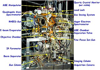
Low-energy electron microscopy, or LEEM, is an analytical surface science technique used to image atomically clean surfaces, atom-surface interactions, and thin (crystalline) films. In LEEM, high-energy electrons are emitted from an electron gun, focused using a set of condenser optics, and sent through a magnetic beam deflector. The “fast” electrons travel through an objective lens and begin decelerating to low energies near the sample surface because the sample is held at a potential near that of the gun. The low-energy electrons are now termed “surface-sensitive” and the near-surface sampling depth can be varied by tuning the energy of the incident electrons. The low-energy elastically backscattered electrons travel back through the objective lens, reaccelerate to the gun voltage, and pass through the beam separator again. However, now the electrons travel away from the condenser optics and into the projector lenses. Imaging of the back focal plane of the objective lens into the object plane of the projector lens produces a diffraction pattern at the imaging plane and recorded in a number of different ways. The intensity distribution of the diffraction pattern will depend on the periodicity at the sample surface and is a direct result of the wave nature of the electrons. One can produce individual images of the diffraction pattern spot intensities by turning off the intermediate lens and inserting a contrast aperture in the back focal plane of the objective lens, thus allowing for real-time observations of dynamic processes at surfaces. Such phenomena include : tomography, phase transitions, adsorption, reaction, segregation, thin film growth, etching, strain relief, sublimation, and magnetic microstructure. These investigations are only possible because of the accessibility of the sample; allowing for a wide variety of in situ studies over a wide temperature range. LEEM was invented by Ernst Bauer in 1962; however, not fully developed until 1985.

Explorer 54, also known as AE-D, was a NASA scientific satellite belonging to the Atmosphere Explorer series launched on 6 October 1975 from Vandenberg Air Force Base aboard a Thor-Delta 2910 launch vehicle.

Instrumental analysis is a field of analytical chemistry that investigates analytes using scientific instruments.
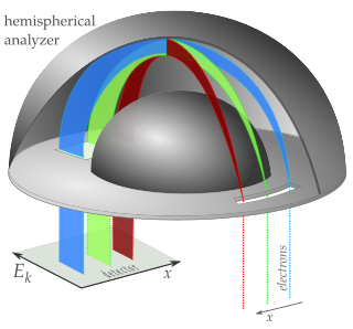
A hemispherical electron energy analyzer or hemispherical deflection analyzer is a type of electron energy spectrometer generally used for applications where high energy resolution is needed—different varieties of electron spectroscopy such as angle-resolved photoemission spectroscopy (ARPES), X-ray photoelectron spectroscopy (XPS) and Auger electron spectroscopy (AES) or in imaging applications such as photoemission electron microscopy (PEEM) and low-energy electron microscopy (LEEM).
Nano Angle-Resolved Photoemission Spectroscopy (Nano-ARPES), is a variant of the experimental technique ARPES. It has the ability to precisely determine the electronic band structure of materials in momentum space with submicron lateral resolution. Due to its demanding experimental setup, this technique is much less extended than ARPES, widely used in condensed matter physics to experimentally determine the electronic properties of a broad range of crystalline materials. Nano-ARPES can access the electronic structure of well-ordered monocrystalline solids with high energy, momentum, and lateral resolution, even if they are nanometric or heterogeneous mesoscopic samples. Nano-ARPES technique is also based on Einstein's photoelectric effect, being photon-in electron-out spectroscopy, which has converted into an essential tool in studying the electronic structure of nanomaterials, like quantum and low dimensional materials.