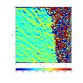
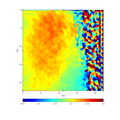
Geometric phase analysis

Last updated
Geometric phase analysis performed by CrysTBox gpaGUI showing input image (bottom left) and d-spacing map (bottom right) GpaGUI.png
Geometric phase analysis performed by CrysTBox gpaGUI showing input image (bottom left) and d-spacing map (bottom right)

Geometric phase analysis is a method of digital signal processing used to determine crystallographic quantities such as d-spacing or strain from high-resolution transmission electron microscope images. [1] [2] The analysis needs to be performed using specialized computer program.

Contents

Principle

In geometric phase analysis, crystallographic quantities are not determined at one particular point of the input image. Instead, they are quantified across the whole image resulting in a two-dimensional map of given quantity. Quantities which can be mapped with geometric phase analysis include interplanar distances (d-spacing), strain tensor and displacement vector.

Since the calculations are performed in frequential domain, the input image of crystal lattice must be transformed into frequential representation using Fourier transform. From mathematical point of view, the frequential image is a complex matrix with the size equal to the original image. From crystallographic point of view, it can be seen as an artificial diffraction pattern or reciprocal image as it depicts reciprocal lattice. In this representation, the intensity peaks (or power peaks) correspond to the crystallographic planes depicted in the original image.

Due to the complex nature of the frequential image, it can be used to calculate amplitude and phase. Together with a vector of one crystallographic plane depicted in the image, the amplitude and phase can be used to generate a 2D map of d-spacing. [1] If two vectors of non-parallel planes are known, the method can be used to generate maps of strain and displacement. [2]

Software

In order to perform geometric phase analysis, a computer tool is needed. Firstly, because manual evaluation of transforms between spatial and frequential domain would be highly impractical. Secondly, a vector of crystallographic plane is an important input parameter and the analysis is sensitive to the accuracy of its localization. Therefore, the accuracy and repeatability of the analysis can be increased by an automated localization of diffraction spots.

The required functionalities are available in crystallographic suite CrysTBox. It offers an interactive implementation geometric phase analysis called gpaGUI. Within gpaGUI, it is possible to index the diffraction spots and localize them with sub-pixel precision using an automated tool diffractGUI. [3]

See also

Related Research Articles

<span class="mw-page-title-main">Crystallography</span> Scientific study of crystal structures

Crystallography is the experimental science of determining the arrangement of atoms in crystalline solids. Crystallography is a fundamental subject in the fields of materials science and solid-state physics. The word crystallography is derived from the Ancient Greek word κρύσταλλος, with its meaning extending to all solids with some degree of transparency, and γράφειν. In July 2012, the United Nations recognised the importance of the science of crystallography by proclaiming that 2014 would be the International Year of Crystallography.

<span class="mw-page-title-main">X-ray crystallography</span> Technique used for determining crystal structures and identifying mineral compounds

X-ray crystallography is the experimental science determining the atomic and molecular structure of a crystal, in which the crystalline structure causes a beam of incident X-rays to diffract into many specific directions. By measuring the angles and intensities of these diffracted beams, a crystallographer can produce a three-dimensional picture of the density of electrons within the crystal. From this electron density, the mean positions of the atoms in the crystal can be determined, as well as their chemical bonds, their crystallographic disorder, and various other information.

<span class="mw-page-title-main">Transmission electron microscopy</span> Technique in microscopy

Transmission electron microscopy (TEM) is a microscopy technique in which a beam of electrons is transmitted through a specimen to form an image. The specimen is most often an ultrathin section less than 100 nm thick or a suspension on a grid. An image is formed from the interaction of the electrons with the sample as the beam is transmitted through the specimen. The image is then magnified and focused onto an imaging device, such as a fluorescent screen, a layer of photographic film, or a sensor such as a scintillator attached to a charge-coupled device.

<span class="mw-page-title-main">Electron diffraction</span> Bending of electron beams due to electrostatic interactions with matter

Electron diffraction refers to changes in the direction of electron beams due to interactions with atoms. Close to the atoms the changes are described as Fresnel diffraction; far away they are called Fraunhofer diffraction. The resulting map of the directions of the electrons far from the sample is called a diffraction pattern, see for instance Figure 1. These patterns are similar to x-ray and neutron diffraction patterns, and are used to study the atomic structure of gases, liquids, surfaces and bulk solids. Electron diffraction also plays a major role in the contrast of images in electron microscopes.

<span class="mw-page-title-main">Electron backscatter diffraction</span> Scanning electron microscopy technique

Electron backscatter diffraction (EBSD) is a scanning electron microscopy (SEM) technique used to study the crystallographic structure of materials. EBSD is carried out in a scanning electron microscope equipped with an EBSD detector comprising at least a phosphorescent screen, a compact lens and a low-light camera. In this configuration, the SEM incident beam hits the tilted sample. As backscattered electrons leave the sample, they interact with the crystal's periodic atomic lattice planes and diffract according to Bragg's law at various scattering angles before reaching the phosphor screen forming Kikuchi patterns (EBSPs). EBSD spatial resolution depends on many factors, including the nature of the material under study and the sample preparation. Thus, EBSPs can be indexed to provide information about the material's grain structure, grain orientation, and phase at the micro-scale. EBSD is applied for impurities and defect studies, plastic deformation, and statistical analysis for average misorientation, grain size, and crystallographic texture. EBSD can also be combined with energy-dispersive X-ray spectroscopy (EDS), cathodoluminescence (CL), and wavelength-dispersive X-ray spectroscopy (WDS) for advanced phase identification and materials discovery.

Electron crystallography is a method to determine the arrangement of atoms in solids using a transmission electron microscope (TEM). It can involve the use of high-resolution transmission electron microscopy images, electron diffraction patterns including convergent-beam electron diffraction or combinations of these. It has been successful in determining some bulk structures, and also surface structures. Two related methods are low-energy electron diffraction which has solved the structure of many surfaces, and reflection high-energy electron diffraction which is used to monitor surfaces often during growth.

<span class="mw-page-title-main">Powder diffraction</span>

Powder diffraction is a scientific technique using X-ray, neutron, or electron diffraction on powder or microcrystalline samples for structural characterization of materials. An instrument dedicated to performing such powder measurements is called a powder diffractometer.

<span class="mw-page-title-main">Selected area diffraction</span>

Selected area (electron) diffraction, is a crystallographic experimental technique typically performed using a transmission electron microscope (TEM). It is a specific case of electron diffraction used primarily in material science and solid state physics as one of the most common experimental techniques. Especially with appropriate analytical software, SAD patterns (SADP) can be used to determine crystal orientation, measure lattice constants or examine its defects.

<span class="mw-page-title-main">High-resolution transmission electron microscopy</span>

High-resolution transmission electron microscopy is an imaging mode of specialized transmission electron microscopes that allows for direct imaging of the atomic structure of samples. It is a powerful tool to study properties of materials on the atomic scale, such as semiconductors, metals, nanoparticles and sp2-bonded carbon. While this term is often also used to refer to high resolution scanning transmission electron microscopy, mostly in high angle annular dark field mode, this article describes mainly the imaging of an object by recording the two-dimensional spatial wave amplitude distribution in the image plane, similar to a "classic" light microscope. For disambiguation, the technique is also often referred to as phase contrast transmission electron microscopy, although this term is less appropriate. At present, the highest point resolution realised in high resolution transmission electron microscopy is around 0.5 ångströms (0.050 nm). At these small scales, individual atoms of a crystal and defects can be resolved. For 3-dimensional crystals, it is necessary to combine several views, taken from different angles, into a 3D map. This technique is called electron tomography.

Electron holography is holography with electron matter waves. Dennis Gabor invented holography in 1948 when he tried to improve image resolution in electron microscope. The first attempts to perform holography with electron waves were made by Haine and Mulvey in 1952; they recorded holograms of zinc oxide crystals with 60 keV electrons, demonstrating reconstructions with approximately 1 nm resolution. In 1955, G. Möllenstedt and H. Düker invented an electron biprism, thus enabling the recording of electron holograms in off-axis scheme. There are many different possible configurations for electron holography, with more than 20 documented in 1992 by Cowley. Usually, high spatial and temporal coherence of the electron beam are required to perform holographic measurements.

<span class="mw-page-title-main">Dark-field microscopy</span> Laboratory technique

Dark-field microscopy describes microscopy methods, in both light and electron microscopy, which exclude the unscattered beam from the image. As a result, the field around the specimen is generally dark.

<span class="mw-page-title-main">Coherent diffraction imaging</span>

Coherent diffractive imaging (CDI) is a "lensless" technique for 2D or 3D reconstruction of the image of nanoscale structures such as nanotubes, nanocrystals, porous nanocrystalline layers, defects, potentially proteins, and more. In CDI, a highly coherent beam of X-rays, electrons or other wavelike particle or photon is incident on an object.

<span class="mw-page-title-main">Kikuchi lines (physics)</span> Patterns formed by scattering

Kikuchi lines are patterns of electrons formed by scattering. They pair up to form bands in electron diffraction from single crystal specimens, there to serve as "roads in orientation-space" for microscopists uncertain of what they are looking at. In transmission electron microscopes, they are easily seen in diffraction from regions of the specimen thick enough for multiple scattering. Unlike diffraction spots, which blink on and off as one tilts the crystal, Kikuchi bands mark orientation space with well-defined intersections as well as paths connecting one intersection to the next.

A crystallographic database is a database specifically designed to store information about the structure of molecules and crystals. Crystals are solids having, in all three dimensions of space, a regularly repeating arrangement of atoms, ions, or molecules. They are characterized by symmetry, morphology, and directionally dependent physical properties. A crystal structure describes the arrangement of atoms, ions, or molecules in a crystal.

<span class="mw-page-title-main">Ptychography</span>

Ptychography is a computational method of microscopic imaging. It generates images by processing many coherent interference patterns that have been scattered from an object of interest. Its defining characteristic is translational invariance, which means that the interference patterns are generated by one constant function moving laterally by a known amount with respect to another constant function. The interference patterns occur some distance away from these two components, so that the scattered waves spread out and "fold" into one another as shown in the figure.

<span class="mw-page-title-main">Crystallographic image processing</span>

Crystallographic image processing (CIP) is traditionally understood as being a set of key steps in the determination of the atomic structure of crystalline matter from high-resolution electron microscopy (HREM) images obtained in a transmission electron microscope (TEM) that is run in the parallel illumination mode. The term was created in the research group of Sven Hovmöller at Stockholm University during the early 1980s and became rapidly a label for the "3D crystal structure from 2D transmission/projection images" approach. Since the late 1990s, analogous and complementary image processing techniques that are directed towards the achieving of goals with are either complementary or entirely beyond the scope of the original inception of CIP have been developed independently by members of the computational symmetry/geometry, scanning transmission electron microscopy, scanning probe microscopy communities, and applied crystallography communities.

Electron channelling contrast imaging (ECCI) is a scanning electron microscope (SEM) diffraction technique used in the study of defects in materials. These can be dislocations or stacking faults that are close to the surface of the sample, low angle grain boundaries or atomic steps. Unlike the use of transmission electron microscopy (TEM) for the investigation of dislocations, the ECCI approach has been called a rapid and non-destructive characterisation technique

<span class="mw-page-title-main">CrysTBox</span> Free crystallographic software

CrysTBox is a suite of computer tools designed to accelerate material research based on transmission electron microscope images via highly accurate automated analysis and interactive visualization. Relying on artificial intelligence and computer vision, CrysTBox makes routine crystallographic analyses simpler, faster and more accurate compared to human evaluators. The high level of automation together with sub-pixel precision and interactive visualization makes the quantitative crystallographic analysis accessible even for non-crystallographers allowing for an interdisciplinary research. Simultaneously, experienced material scientists can take advantage of advanced functionalities for comprehensive analyses.

4D scanning transmission electron microscopy is a subset of scanning transmission electron microscopy (STEM) which utilizes a pixelated electron detector to capture a convergent beam electron diffraction (CBED) pattern at each scan location. This technique captures a 2 dimensional reciprocal space image associated with each scan point as the beam rasters across a 2 dimensional region in real space, hence the name 4D STEM. Its development was enabled by evolution in STEM detectors and improvements computational power. The technique has applications in visual diffraction imaging, phase orientation and strain mapping, phase contrast analysis, among others.

Angus J Wilkinson is a professor of materials science based at University of Oxford. He is a specialist in micromechanics, electron microscopy and crystal plasticity. He assists in overseeing the MicroMechanics group while focusing on the fundamentals of material deformation. He developed the HR-EBSD method for mapping stress and dislocation density at high spatial resolution used at the micron scale in mechanical testing and micro-cantilevers to extract data on mechanical properties that are relevant to materials engineering.

References

  1. 1 2 Hÿtch, M.J. (1997). "Geometric phase analysis of high resolution electron microscope images". Scanning Microscopy. 11: 53–66.
  2. 1 2 Hÿtch, M.J.; Snoeck, E.; Kilaas, R. (1998). "Quantitative measurement of displacement and strain fields from HREM micrographs". Ultramicroscopy. Elsevier BV. 74 (3): 131–146. doi:10.1016/s0304-3991(98)00035-7. ISSN   0304-3991.
  3. Klinger, Miloslav (2017-07-07). "More features, more tools, more CrysTBox". Journal of Applied Crystallography. International Union of Crystallography (IUCr). 50 (4): 1226–1234. doi:10.1107/s1600576717006793. ISSN   1600-5767.