
A printed circuit board (PCB) is a laminated sandwich structure of conductive and insulating layers. PCBs have two complementary functions. The first is to affix electronic components in designated locations on the outer layers by means of soldering. The second is to provide reliable electrical connections between the component's terminals in a controlled manner often referred to as PCB design. Each of the conductive layers is designed with an artwork pattern of conductors that provides electrical connections on that conductive layer, while another manufacturing process adds vias - small and precisely located holes that are drilled through the laminate and then plated with copper. The vias are the electrical interconnection between layers that are otherwise insulated in the laminate structure and this allows a third dimension of connection between conductive layers in a controlled manner that is both reliable and cost-effective for mass production of electronic products.

Thermal insulation is the reduction of heat transfer between objects in thermal contact or in range of radiative influence. Thermal insulation can be achieved with specially engineered methods or processes, as well as with suitable object shapes and materials.
Radiative cooling is the process by which a body loses heat by thermal radiation. As Planck's law describes, every physical body spontaneously and continuously emits electromagnetic radiation.

Heat transfer is a discipline of thermal engineering that concerns the generation, use, conversion, and exchange of thermal energy (heat) between physical systems. Heat transfer is classified into various mechanisms, such as thermal conduction, thermal convection, thermal radiation, and transfer of energy by phase changes. Engineers also consider the transfer of mass of differing chemical species, either cold or hot, to achieve heat transfer. While these mechanisms have distinct characteristics, they often occur simultaneously in the same system.
Glass-ceramics are polycrystalline materials produced through controlled crystallization of base glass. Glass-ceramic materials share many properties with both glasses and ceramics. Glass-ceramics have an amorphous phase and one or more crystalline phases and are produced by a so-called "controlled crystallization" in contrast to a spontaneous crystallization, which is usually not wanted in glass manufacturing. Glass-ceramics have the fabrication advantage of glass, as well as special properties of ceramics. When used for sealing, some glass-ceramics do not require brazing but can withstand brazing temperatures up to 700 °C. Glass-ceramics usually have between 30% [m/m] and 90% [m/m] crystallinity and yield an array of materials with interesting properties like zero porosity, high strength, toughness, translucency or opacity, pigmentation, opalescence, low or even negative thermal expansion, high temperature stability, fluorescence, machinability, ferromagnetism, resorbability or high chemical durability, biocompatibility, bioactivity, ion conductivity, superconductivity, isolation capabilities, low dielectric constant and loss, high resistivity and break-down voltage. These properties can be tailored by controlling the base-glass composition and by controlled heat treatment/crystallization of base glass. In manufacturing, glass-ceramics are valued for having the strength of ceramic but the hermetic sealing properties of glass.

Lamination is the technique/process of manufacturing a material in multiple layers, so that the composite material achieves improved strength, stability, sound insulation, appearance, or other properties from the use of the differing materials, such as plastic. A laminate is a permanently assembled object created using heat, pressure, welding, or adhesives. Various coating machines, machine presses and calendering equipment are used.

A radiant barrier is a type of building material that reflects thermal radiation and reduces heat transfer. Because thermal energy is also transferred by conduction and convection, in addition radiation, radiant barriers are often supplemented with thermal insulation that slows down heat transfer by conduction or convection.
A thin film is a layer of material ranging from fractions of a nanometer (monolayer) to several micrometers in thickness. The controlled synthesis of materials as thin films is a fundamental step in many applications. A familiar example is the household mirror, which typically has a thin metal coating on the back of a sheet of glass to form a reflective interface. The process of silvering was once commonly used to produce mirrors, while more recently the metal layer is deposited using techniques such as sputtering. Advances in thin film deposition techniques during the 20th century have enabled a wide range of technological breakthroughs in areas such as magnetic recording media, electronic semiconductor devices, Integrated passive devices, LEDs, optical coatings, hard coatings on cutting tools, and for both energy generation and storage. It is also being applied to pharmaceuticals, via thin-film drug delivery. A stack of thin films is called a multilayer.

A heating element converts electrical energy into heat through the process of Joule heating. Electric current through the element encounters resistance, resulting in heating of the element. Unlike the Peltier effect, this process is independent of the direction of current.
A hermetic seal is any type of sealing that makes a given object airtight. The term originally applied to airtight glass containers, but as technology advanced it applied to a larger category of materials, including rubber and plastics. Hermetic seals are essential to the correct and safe functionality of many electronic and healthcare products. Used technically, it is stated in conjunction with a specific test method and conditions of use.
Nanoimprint lithography (NIL) is a method of fabricating nanometer scale patterns. It is a simple nanolithography process with low cost, high throughput and high resolution. It creates patterns by mechanical deformation of imprint resist and subsequent processes. The imprint resist is typically a monomer or polymer formulation that is cured by heat or UV light during the imprinting. Adhesion between the resist and the template is controlled to allow proper release.
The role of the substrate in power electronics is to provide the interconnections to form an electric circuit, and to cool the components. Compared to materials and techniques used in lower power microelectronics, these substrates must carry higher currents and provide a higher voltage isolation. They also must operate over a wide temperature range.

Printed electronics is a set of printing methods used to create electrical devices on various substrates. Printing typically uses common printing equipment suitable for defining patterns on material, such as screen printing, flexography, gravure, offset lithography, and inkjet. By electronic-industry standards, these are low-cost processes. Electrically functional electronic or optical inks are deposited on the substrate, creating active or passive devices, such as thin film transistors; capacitors; coils; resistors. Some researchers expect printed electronics to facilitate widespread, very low-cost, low-performance electronics for applications such as flexible displays, smart labels, decorative and animated posters, and active clothing that do not require high performance.
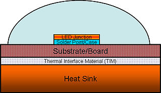
High power light-emitting diodes (LEDs) can use 350 milliwatts or more in a single LED. Most of the electricity in an LED becomes heat rather than light. If this heat is not removed, the LEDs run at high temperatures, which not only lowers their efficiency, but also makes the LED less reliable. Thus, thermal management of high power LEDs is a crucial area of research and development. It is necessary to limit both the junction and the phosphor particles temperatures to a value that will guarantee the desired LED lifetime.

The thermal copper pillar bump, also known as the "thermal bump", is a thermoelectric device made from thin-film thermoelectric material embedded in flip chip interconnects for use in electronics and optoelectronic packaging, including: flip chip packaging of CPU and GPU integrated circuits (chips), laser diodes, and semiconductor optical amplifiers (SOA). Unlike conventional solder bumps that provide an electrical path and a mechanical connection to the package, thermal bumps act as solid-state heat pumps and add thermal management functionality locally on the surface of a chip or to another electrical component. The diameter of a thermal bump is 238 μm and 60 μm high.

Thick-film technology is used to produce electronic devices/modules such as surface mount devices modules, hybrid integrated circuits, heating elements, integrated passive devices and sensors. Main manufacturing technique is screen printing (stenciling), which in addition to use in manufacturing electronic devices can also be used for various graphic reproduction targets. The technique is known in its basic form about thousand years – already used during great Chinese dynasties. It became one of the key manufacturing/miniaturisation techniques of electronic devices/modules during 1950s. Typical film thickness – manufactured with thick film manufacturing processes for electronic devices – is 0.0001 to 0.1 mm.
Hot pressing is a high-pressure, low-strain-rate powder metallurgy process for forming of a powder or powder compact at a temperature high enough to induce sintering and creep processes. This is achieved by the simultaneous application of heat and pressure.

Selective laser melting (SLM) is one of many proprietary names for a metal additive manufacturing technology that uses a bed of powder with a source of heat to create metal parts. Also known as direct metal laser melting (DMLM), the ASTM standard term is powder bed fusion (PBF). PBF is a rapid prototyping, 3D printing, or additive manufacturing (AM) technique designed to use a high power-density laser to melt and fuse metallic powders together.

Inkjet technology originally was invented for depositing aqueous inks on paper in 'selective' positions based on the ink properties only. Inkjet nozzles and inks were designed together and the inkjet performance was based on a design. It was used as a data recorder in the early 1950s, later in the 1950s co-solvent-based inks in the publishing industry were seen for text and images, then solvent-based inks appeared in industrial marking on specialized surfaces and in the1990's phase change or hot-melt ink has become a popular with images and digital fabrication of electronic and mechanical devices, especially jewelry. Although the terms "jetting", "inkjet technology" and "inkjet printing", are commonly used interchangeably, inkjet printing usually refers to the publishing industry, used for printing graphical content, while industrial jetting usually refers to general purpose fabrication via material particle deposition.
Three-dimensional (3D) microfabrication refers to manufacturing techniques that involve the layering of materials to produce a three-dimensional structure at a microscopic scale. These structures are usually on the scale of micrometers and are popular in microelectronics and microelectromechanical systems.