Microelectromechanical systems (MEMS), also written as micro-electro-mechanical systems and the related micromechatronics and microsystems constitute the technology of microscopic devices, particularly those with moving parts. They merge at the nanoscale into nanoelectromechanical systems (NEMS) and nanotechnology. MEMS are also referred to as micromachines in Japan and microsystem technology (MST) in Europe.
In integrated circuit manufacturing, photolithography or optical lithography is a general term used for techniques that use light to produce minutely patterned thin films of suitable materials over a substrate, such as a silicon wafer, to protect selected areas of it during subsequent etching, deposition, or implantation operations. Typically, ultraviolet light is used to transfer a geometric design from an optical mask to a light-sensitive chemical (photoresist) coated on the substrate. The photoresist either breaks down or hardens where it is exposed to light. The patterned film is then created by removing the softer parts of the coating with appropriate solvents.
In physics, sputtering is a phenomenon in which microscopic particles of a solid material are ejected from its surface, after the material is itself bombarded by energetic particles of a plasma or gas. It occurs naturally in outer space, and can be an unwelcome source of wear in precision components. However, the fact that it can be made to act on extremely fine layers of material is utilised in science and industry—there, it is used to perform precise etching, carry out analytical techniques, and deposit thin film layers in the manufacture of optical coatings, semiconductor devices and nanotechnology products. It is a physical vapor deposition technique.
Inductively coupled plasma mass spectrometry (ICP-MS) is a type of mass spectrometry that uses an inductively coupled plasma to ionize the sample. It atomizes the sample and creates atomic and small polyatomic ions, which are then detected. It is known and used for its ability to detect metals and several non-metals in liquid samples at very low concentrations. It can detect different isotopes of the same element, which makes it a versatile tool in isotopic labeling.
An inductively coupled plasma (ICP) or transformer coupled plasma (TCP) is a type of plasma source in which the energy is supplied by electric currents which are produced by electromagnetic induction, that is, by time-varying magnetic fields.
Dry etching refers to the removal of material, typically a masked pattern of semiconductor material, by exposing the material to a bombardment of ions that dislodge portions of the material from the exposed surface. A common type of dry etching is reactive-ion etching. Unlike with many of the wet chemical etchants used in wet etching, the dry etching process typically etches directionally or anisotropically.

An ion beam is a type of charged particle beam consisting of ions. Ion beams have many uses in electronics manufacturing and other industries. A variety of ion beam sources exists, some derived from the mercury vapor thrusters developed by NASA in the 1960s. The most common ion beams are of singly-charged ions.
Deep reactive-ion etching (DRIE) is a highly anisotropic etch process used to create deep penetration, steep-sided holes and trenches in wafers/substrates, typically with high aspect ratios. It was developed for microelectromechanical systems (MEMS), which require these features, but is also used to excavate trenches for high-density capacitors for DRAM and more recently for creating through silicon vias (TSVs) in advanced 3D wafer level packaging technology. In DRIE, the substrate is placed inside a reactor, and several gases are introduced. A plasma is struck in the gas mixture which breaks the gas molecules into ions. The ions accelerated towards, and react with the surface of the material being etched, forming another gaseous element. This is known as the chemical part of the reactive ion etching. There is also a physical part, if ions have enough energy, they can knock atoms out of the material to be etched without chemical reaction.
A capacitively coupled plasma (CCP) is one of the most common types of industrial plasma sources. It essentially consists of two metal electrodes separated by a small distance, placed in a reactor. The gas pressure in the reactor can be lower than atmosphere or it can be atmospheric.

Microfabrication is the process of fabricating miniature structures of micrometre scales and smaller. Historically, the earliest microfabrication processes were used for integrated circuit fabrication, also known as "semiconductor manufacturing" or "semiconductor device fabrication". In the last two decades microelectromechanical systems (MEMS), microsystems, micromachines and their subfields, microfluidics/lab-on-a-chip, optical MEMS, RF MEMS, PowerMEMS, BioMEMS and their extension into nanoscale have re-used, adapted or extended microfabrication methods. Flat-panel displays and solar cells are also using similar techniques.

Inductively coupled plasma atomic emission spectroscopy (ICP-AES), also referred to as inductively coupled plasma optical emission spectroscopy (ICP-OES), is an analytical technique used for the detection of chemical elements. It is a type of emission spectroscopy that uses the inductively coupled plasma to produce excited atoms and ions that emit electromagnetic radiation at wavelengths characteristic of a particular element. The plasma is a high temperature source of ionised source gas. The plasma is sustained and maintained by inductive coupling from electrical coils at megahertz frequencies. The source temperature is in the range from 6000 to 10,000 K. The intensity of the emissions from various wavelengths of light are proportional to the concentrations of the elements within the sample.
Plasma etching is a form of plasma processing used to fabricate integrated circuits. It involves a high-speed stream of glow discharge (plasma) of an appropriate gas mixture being shot at a sample. The plasma source, known as etch species, can be either charged (ions) or neutral. During the process, the plasma generates volatile etch products at room temperature from the chemical reactions between the elements of the material etched and the reactive species generated by the plasma. Eventually the atoms of the shot element embed themselves at or just below the surface of the target, thus modifying the physical properties of the target.
Advanced silicon etching (ASE) is a deep reactive-ion etching (DRIE) technique to etch deep and high aspect ratio structures in silicon. ASE was created by Surface Technology Systems Plc (STS) in 1994 in the UK. STS has continued to develop this process with faster etch rates. STS developed and first implemented the switched process, originally invented by Dr. Larmer in Bosch, Stuttgart. ASE consists in combining the faster etch rates achieved in an isotropic Si etch (usually making use of an SF6 plasma) with a deposition or passivation process (usually utilising a C4F8 plasma condensation process) by alternating the two process steps. This approach achieves the fastest etch rates while maintaining the ability to etch anisotropically, typically vertically in Microelectromechanical Systems (microelectromechanical systems (MEMS)) applications.

Plasma-enhanced chemical vapor deposition (PECVD) is a chemical vapor deposition process used to deposit thin films from a gas state (vapor) to a solid state on a substrate. Chemical reactions are involved in the process, which occur after creation of a plasma of the reacting gases. The plasma is generally created by radio frequency (RF) frequency or direct current (DC) discharge between two electrodes, the space between which is filled with the reacting gases.

Etching is used in microfabrication to chemically remove layers from the surface of a wafer during manufacturing. Etching is a critically important process module, and every wafer undergoes many etching steps before it is complete.

Sputter deposition is a physical vapor deposition (PVD) method of thin film deposition by the phenomenon of sputtering. This involves ejecting material from a "target" that is a source onto a "substrate" such as a silicon wafer. Resputtering is re-emission of the deposited material during the deposition process by ion or atom bombardment. Sputtered atoms ejected from the target have a wide energy distribution, typically up to tens of eV. The sputtered ions can ballistically fly from the target in straight lines and impact energetically on the substrates or vacuum chamber. Alternatively, at higher gas pressures, the ions collide with the gas atoms that act as a moderator and move diffusively, reaching the substrates or vacuum chamber wall and condensing after undergoing a random walk. The entire range from high-energy ballistic impact to low-energy thermalized motion is accessible by changing the background gas pressure. The sputtering gas is often an inert gas such as argon. For efficient momentum transfer, the atomic weight of the sputtering gas should be close to the atomic weight of the target, so for sputtering light elements neon is preferable, while for heavy elements krypton or xenon are used. Reactive gases can also be used to sputter compounds. The compound can be formed on the target surface, in-flight or on the substrate depending on the process parameters. The availability of many parameters that control sputter deposition make it a complex process, but also allow experts a large degree of control over the growth and microstructure of the film.
Alcatel Micro Machining Systems (AMMS) was a French manufacturer of Deep Reactive Ion Etching systems. The company's headquarters were located in Annecy, France.

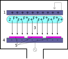
Plasma-immersion ion implantation (PIII) or pulsed-plasma doping is a surface modification technique of extracting the accelerated ions from the plasma by applying a high voltage pulsed DC or pure DC power supply and targeting them into a suitable substrate or electrode with a semiconductor wafer placed over it, so as to implant it with suitable dopants. The electrode is a cathode for an electropositive plasma, while it is an anode for an electronegative plasma. Plasma can be generated in a suitably designed vacuum chamber with the help of various plasma sources such as electron cyclotron resonance plasma source which yields plasma with the highest ion density and lowest contamination level, helicon plasma source, capacitively coupled plasma source, inductively coupled plasma source, DC glow discharge and metal vapor arc. The vacuum chamber can be of two types - diode and triode type depending upon whether the power supply is applied to the substrate as in the former case or to the perforated grid as in the latter.
Black silicon is a semiconductor material, a surface modification of silicon with very low reflectivity and correspondingly high absorption of visible light.
Plasma-activated bonding is a derivative, directed to lower processing temperatures for direct bonding with hydrophilic surfaces. The main requirements for lowering temperatures of direct bonding are the use of materials melting at low temperatures and with different coefficients of thermal expansion (CTE).