Semiconductor device modeling

Last updated

Hierarchy of technology CAD tools building from the process level to circuits. Left side icons show typical manufacturing issues; right side icons reflect MOS scaling results based on TCAD. Credit: Prof. Robert Dutton in CRC Electronic Design Automation for IC Handbook, Vol II, Chapter 25, by permission. TCAD-overview.JPG
Hierarchy of technology CAD tools building from the process level to circuits. Left side icons show typical manufacturing issues; right side icons reflect MOS scaling results based on TCAD. Credit: Prof. Robert Dutton in CRC Electronic Design Automation for IC Handbook, Vol II, Chapter 25, by permission.

Semiconductor device modeling creates models for the behavior of the electrical devices based on fundamental physics, such as the doping profiles of the devices. It may also include the creation of compact models (such as the well known SPICE transistor models), which try to capture the electrical behavior of such devices but do not generally derive them from the underlying physics. Normally it starts from the output of a semiconductor process simulation.

Contents

Introduction

Schematic of two stages of CMOS inverter, showing input and output voltage-time plots. Ion and Ioff (along with IDG, ISD and IDB components) indicate technologically controlled factors. Credit: Prof. Robert Dutton in CRC Electronic Design Automation for IC Handbook, Vol II, Chapter 25, by permission. TCAD-circuit.jpg
Schematic of two stages of CMOS inverter, showing input and output voltage-time plots. Ion and Ioff (along with IDG, ISD and IDB components) indicate technologically controlled factors. Credit: Prof. Robert Dutton in CRC Electronic Design Automation for IC Handbook, Vol II, Chapter 25, by permission.

The figure to the right provides a simplified conceptual view of “the big picture.” This figure shows two inverter stages and the resulting input-output voltage-time plot of the circuit. From the digital systems point of view the key parameters of interest are: timing delays, switching power, leakage current and cross-coupling (crosstalk) with other blocks. The voltage levels and transition speed are also of concern.

The figure also shows schematically the importance of Ion versus Ioff, which in turn is related to drive-current (and mobility) for the “on” device and several leakage paths for the “off” devices. Not shown explicitly in the figure are the capacitances—both intrinsic and parasitic—that affect dynamic performance.

The power scaling which is now a major driving force in the industry is reflected in the simplified equation shown in the figure — critical parameters are capacitance, power supply and clocking frequency. Key parameters that relate device behavior to system performance include the threshold voltage, driving current and subthreshold characteristics.

It is the confluence of system performance issues with the underlying technology and device design variables that results in the ongoing scaling laws that we now codify as Moore’s law.

Device modeling

The physics and modeling of devices in integrated circuits is dominated by MOS and bipolar transistor modeling. However, other devices are important, such as memory devices, that have rather different modeling requirements. There are of course also issues of reliability engineering—for example, electro-static discharge (ESD) protection circuits and devices—where substrate and parasitic devices are of pivotal importance. These effects and modeling are not considered by most device modeling programs; the interested reader is referred to several excellent monographs in the area of ESD and I/O modeling. [1] [2] [3]

Physics driven vs. compact models

An example of physics driven modeling of a MOSFET. The color contours indicate space resolved local density of states. Gate bias is varied in a nanowire MOSFET at drain bias Vd=0.6V. Notice the confined energy levels as they move with gate bias. Omen ldos v3.gif
An example of physics driven modeling of a MOSFET. The color contours indicate space resolved local density of states. Gate bias is varied in a nanowire MOSFET at drain bias Vd=0.6V. Notice the confined energy levels as they move with gate bias.

Physics driven device modeling is intended to be accurate, but it is not fast enough for higher level tools, including circuit simulators such as SPICE. Therefore, circuit simulators normally use more empirical models (often called compact models) that do not directly model the underlying physics. For example, inversion-layer mobility modeling, or the modeling of mobility and its dependence on physical parameters, ambient and operating conditions is an important topic both for TCAD (technology computer aided design) physical models and for circuit-level compact models. However, it is not accurately modeled from first principles, and so resort is taken to fitting experimental data. For mobility modeling at the physical level the electrical variables are the various scattering mechanisms, carrier densities, and local potentials and fields, including their technology and ambient dependencies.

By contrast, at the circuit-level, models parameterize the effects in terms of terminal voltages and empirical scattering parameters. The two representations can be compared, but it is unclear in many cases how the experimental data is to be interpreted in terms of more microscopic behavior.

History

The evolution of technology computer-aided design (TCAD)--the synergistic combination of process, device and circuit simulation and modeling tools—finds its roots in bipolar technology, starting in the late 1960s, and the challenges of junction isolated, double-and triple-diffused transistors. These devices and technology were the basis of the first integrated circuits; nonetheless, many of the scaling issues and underlying physical effects are integral to IC design, even after four decades of IC development. With these early generations of IC, process variability and parametric yield were an issue—a theme that will reemerge as a controlling factor in future IC technology as well.

Process control issues—both for the intrinsic devices and all the associated parasitics—presented formidable challenges and mandated the development of a range of advanced physical models for process and device simulation. Starting in the late 1960s and into the 1970s, the modeling approaches exploited were dominantly one- and two-dimensional simulators. While TCAD in these early generations showed exciting promise in addressing the physics-oriented challenges of bipolar technology, the superior scalability and power consumption of MOS technology revolutionized the IC industry. By the mid-1980s, CMOS became the dominant driver for integrated electronics. Nonetheless, these early TCAD developments [4] [5] set the stage for their growth and broad deployment as an essential toolset that has leveraged technology development through the VLSI and ULSI eras which are now the mainstream.

IC development for more than a quarter-century has been dominated by the MOS technology. In the 1970s and 1980s NMOS was favored owing to speed and area advantages, coupled with technology limitations and concerns related to isolation, parasitic effects and process complexity. During that era of NMOS-dominated LSI and the emergence of VLSI, the fundamental scaling laws of MOS technology were codified and broadly applied. [6] It was also during this period that TCAD reached maturity in terms of realizing robust process modeling (primarily one-dimensional) which then became an integral technology design tool, used universally across the industry. [7] At the same time device simulation, dominantly two-dimensional owing to the nature of MOS devices, became the work-horse of technologists in the design and scaling of devices. [8] [9] The transition from NMOS to CMOS technology resulted in the necessity of tightly coupled and fully 2D simulators for process and device simulations. This third generation of TCAD tools became critical to address the full complexity of twin-well CMOS technology (see Figure 3a), including issues of design rules and parasitic effects such as latchup. [10] [11] An abbreviated perspective of this period, through the mid-1980s, is given in; [12] and from the point of view of how TCAD tools were used in the design process, see. [13]

See also

Related Research Articles

<span class="mw-page-title-main">Integrated circuit</span> Electronic circuit formed on a small, flat piece of semiconductor material

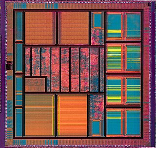
An integrated circuit (IC), also known as a microchip, computer chip, or simply chip, is a small electronic device made up of multiple interconnected electronic components such as transistors, resistors, and capacitors. These components are etched onto a small piece of semiconductor material, usually silicon. Integrated circuits are used in a wide range of electronic devices, including computers, smartphones, and televisions, to perform various functions such as processing and storing information. They have greatly impacted the field of electronics by enabling device miniaturization and enhanced functionality.

<span class="mw-page-title-main">Very-large-scale integration</span> Creating an integrated circuit by combining many transistors into a single chip

Very-large-scale integration (VLSI) is the process of creating an integrated circuit (IC) by combining millions or billions of MOS transistors onto a single chip. VLSI began in the 1970s when MOS integrated circuit chips were developed and then widely adopted, enabling complex semiconductor and telecommunication technologies. The microprocessor and memory chips are VLSI devices.

<span class="mw-page-title-main">MOSFET</span> Type of field-effect transistor

The metal–oxide–semiconductor field-effect transistor is a type of field-effect transistor (FET), most commonly fabricated by the controlled oxidation of silicon. It has an insulated gate, the voltage of which determines the conductivity of the device. This ability to change conductivity with the amount of applied voltage can be used for amplifying or switching electronic signals. The term metal–insulator–semiconductor field-effect transistor (MISFET) is almost synonymous with MOSFET. Another near-synonym is insulated-gate field-effect transistor (IGFET).

<span class="mw-page-title-main">CMOS</span> Technology for constructing integrated circuits

Complementary metal–oxide–semiconductor is a type of metal–oxide–semiconductor field-effect transistor (MOSFET) fabrication process that uses complementary and symmetrical pairs of p-type and n-type MOSFETs for logic functions. CMOS technology is used for constructing integrated circuit (IC) chips, including microprocessors, microcontrollers, memory chips, and other digital logic circuits. CMOS technology is also used for analog circuits such as image sensors, data converters, RF circuits, and highly integrated transceivers for many types of communication.
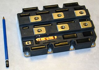
In computer engineering, a logic family is one of two related concepts:

<span class="mw-page-title-main">Mixed-signal integrated circuit</span> Integrated circuit

A mixed-signal integrated circuit is any integrated circuit that has both analog circuits and digital circuits on a single semiconductor die. Their usage has grown dramatically with the increased use of cell phones, telecommunications, portable electronics, and automobiles with electronics and digital sensors.

<span class="mw-page-title-main">Depletion-load NMOS logic</span> Form of digital logic family in integrated circuits

In integrated circuits, depletion-load NMOS is a form of digital logic family that uses only a single power supply voltage, unlike earlier NMOS logic families that needed more than one different power supply voltage. Although manufacturing these integrated circuits required additional processing steps, improved switching speed and the elimination of the extra power supply made this logic family the preferred choice for many microprocessors and other logic elements.

Transistors are simple devices with complicated behavior. In order to ensure the reliable operation of circuits employing transistors, it is necessary to scientifically model the physical phenomena observed in their operation using transistor models. There exists a variety of different models that range in complexity and in purpose. Transistor models divide into two major groups: models for device design and models for circuit design.

<span class="mw-page-title-main">Technology CAD</span>

Technology computer-aided design is a branch of electronic design automation (EDA) that models semiconductor fabrication and semiconductor device operation. The modeling of the fabrication is termed process TCAD, while the modeling of the device operation is termed device TCAD. Included are the modelling of process steps, and modelling of the behavior of the electrical devices based on fundamental physics, such as the doping profiles of the devices. TCAD may also include the creation of "compact models", which try to capture the electrical behavior of such devices but do not generally derive them from the underlying physics. SPICE simulator itself is usually considered as part of EDA rather than TCAD.

<span class="mw-page-title-main">Semiconductor process simulation</span> Modeling for semiconductor fabrication

Semiconductor process simulation is the modeling of the fabrication of semiconductor devices such as transistors. It is a branch of electronic design automation, and part of a sub-field known as technology CAD, or TCAD.

ggNMOS Electrostatic discharge (ESD) protection device

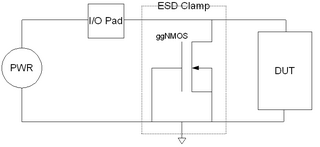
Grounded-gate NMOS, commonly known as ggNMOS, is an electrostatic discharge (ESD) protection device used within CMOS integrated circuits (ICs). Such devices are used to protect the inputs and outputs of an IC, which can be accessed off-chip and are therefore subject to ESD when touched. An ESD event can deliver a large amount of energy to the chip, potentially destroying input/output circuitry; a ggNMOS device or other ESD protective devices provide a safe path for current to flow, instead of through more sensitive circuitry. ESD protection by means of such devices or other techniques is important to product reliability: 35% of all IC failures in the field are associated with ESD damage.

In semiconductor electronics fabrication technology, a self-aligned gate is a transistor manufacturing approach whereby the gate electrode of a MOSFET is used as a mask for the doping of the source and drain regions. This technique ensures that the gate is naturally and precisely aligned to the edges of the source and drain.

<span class="mw-page-title-main">PMOS logic</span> Family of digital circuits

PMOS or pMOS logic is a family of digital circuits based on p-channel, enhancement mode metal–oxide–semiconductor field-effect transistors (MOSFETs). In the late 1960s and early 1970s, PMOS logic was the dominant semiconductor technology for large-scale integrated circuits before being superseded by NMOS and CMOS devices.

<span class="mw-page-title-main">Chih-Tang Sah</span> Chinese-American electronics engineer (born 1932)

Chih-Tang "Tom" Sah is a Chinese-American electronics engineer and condensed matter physicist. He is best known for inventing CMOS logic with Frank Wanlass at Fairchild Semiconductor in 1963. CMOS is used in nearly all modern very large-scale integration (VLSI) semiconductor devices.

In semiconductor manufacturing, a process corner is an example of a design-of-experiments (DoE) technique that refers to a variation of fabrication parameters used in applying an integrated circuit design to a semiconductor wafer. Process corners represent the extremes of these parameter variations within which a circuit that has been etched onto the wafer must function correctly. A circuit running on devices fabricated at these process corners may run slower or faster than specified and at lower or higher temperatures and voltages, but if the circuit does not function at all at any of these process extremes the design is considered to have inadequate design margin.

CoolSPICE is a computer-aided design tool for electronic circuit development. It is a version of the SPICE simulation tool that focuses on design and simulation for circuit operation at cryogenic temperatures, circuits operating with Wide-bandgap semiconductors, and simulation of thermal effects on circuit performance.

Robert W. Dutton is an American electrical engineer. At Stanford University, he is the Robert and Barbara Kleist Professor of Electrical Engineering, Emeritus. Dutton also served as the undergraduate advisor for Stanford University Department of Electrical Engineering, succeeded by John M. Pauly.

RF CMOS is a metal–oxide–semiconductor (MOS) integrated circuit (IC) technology that integrates radio-frequency (RF), analog and digital electronics on a mixed-signal CMOS RF circuit chip. It is widely used in modern wireless telecommunications, such as cellular networks, Bluetooth, Wi-Fi, GPS receivers, broadcasting, vehicular communication systems, and the radio transceivers in all modern mobile phones and wireless networking devices. RF CMOS technology was pioneered by Pakistani engineer Asad Ali Abidi at UCLA during the late 1980s to early 1990s, and helped bring about the wireless revolution with the introduction of digital signal processing in wireless communications. The development and design of RF CMOS devices was enabled by van der Ziel's FET RF noise model, which was published in the early 1960s and remained largely forgotten until the 1990s.

Yuan Taur is a Chinese American electrical engineer and an academic. He is a Distinguished Professor of Electrical and Computer Engineering (ECE) at the University of California, San Diego.

References

  1. C. Duvvury and A. Amerasekera, ESD: a pervasive reliability concern for IC technologies, Proc. IEEE, vol. 81, pp. 690-702, 1993.
  2. A. Amerasekera and C. Duvvury, ESD in Silicon Integrated Circuits, Second Edition, New York, John Wiley & Sons, 2002. ISBN   0-471-49871-8
  3. S. Dabral and T. J. Maloney, Basic ESD and I/O design, New York, John Wiley & Sons, 1998. ISBN   0-471-25359-6
  4. H.J. DeMan and R. Mertens, SITCAP--A simulator for bipolar transistors for computer-aided circuit analysis programs, International Solid-State Circuits Conference (ISSCC), Technical Digest, pp. 104-5, February, 1973.
  5. R.W. Dutton and D.A. Antoniadis, Process simulation for device design and control, International Solid-State Circuits Conference (ISSCC), Technical Digest, pp. 244-245, February, 1979
  6. R.H. Dennard, F.H. Gaensslen, H.N. Yu, V.L. Rodeout, E. Bassous and A.R. LeBlanc, Design of ion-implanted MOSFETs with very small physical dimensions, IEEE Jour. Solid-State Circuits, vol. SC-9, pp.256-268, October, 1974.
  7. R.W. Dutton and S.E. Hansen, Process modeling of integrated circuit device technology, Proceedings of the IEEE, vol. 69, no. 10, pp. 1305-1320, October, 1981.
  8. P.E. Cottrell and E.M. Buturla, "Two-dimensional static and transient simulation of mobile carrier transport in a semiconductor," Proceedings NASECODE I (Numerical Analysis of Semiconductor Devices), pp. 31-64, Boole Press, 1979.
  9. S. Selberherr, W. Fichtner, and H.W. Potzl, "Minimos - A program package to facilitate MOS device design and analysis," Proceedings NASECODE I (Numerical Analysis of Semiconductor Devices), pp. 275-79, Boole Press, 1979.
  10. C.S. Rafferty, M.R. Pinto, and R.W. Dutton, Iterative methods in semiconductor device simulation, IEEE Trans. Elec. Dev., vol. ED-32, no.10, pp.2018-2027, October, 1985.
  11. M.R. Pinto and R.W. Dutton, Accurate trigger condition analysis for CMOS latchup, IEEE Electron Device Letters, vol. EDL-6, no. 2, February, 1985.
  12. R.W. Dutton, Modeling and simulation for VLSI, International Electron Devices Meeting (IEDM), Technical Digest, pp. 2-7, December, 1986.
  13. K.M. Cham, S.-Y. Oh, D. Chin and J.L. Moll, Computer-Aided Design and VLSI Device Development, Kluwer Academic Publishers (KAP), 1986. ISBN   0-89838-204-1