Magnetoresistance is the tendency of a material to change the value of its electrical resistance in an externally-applied magnetic field. There are a variety of effects that can be called magnetoresistance. Some occur in bulk non-magnetic metals and semiconductors, such as geometrical magnetoresistance, Shubnikov–de Haas oscillations, or the common positive magnetoresistance in metals. Other effects occur in magnetic metals, such as negative magnetoresistance in ferromagnets or anisotropic magnetoresistance (AMR). Finally, in multicomponent or multilayer systems, giant magnetoresistance (GMR), tunnel magnetoresistance (TMR), colossal magnetoresistance (CMR), and extraordinary magnetoresistance (EMR) can be observed.

Ohm's law states that the current through a conductor between two points is directly proportional to the voltage across the two points. Introducing the constant of proportionality, the resistance, one arrives at the usual mathematical equation that describes this relationship:
The quantum Hall effect is a quantized version of the Hall effect which is observed in two-dimensional electron systems subjected to low temperatures and strong magnetic fields, in which the Hall resistance Rxy exhibits steps that take on the quantized values

The electrical resistance of an object is a measure of its opposition to the flow of electric current. Its reciprocal quantity is electrical conductance, measuring the ease with which an electric current passes. Electrical resistance shares some conceptual parallels with mechanical friction. The SI unit of electrical resistance is the ohm, while electrical conductance is measured in siemens (S).
Electrical resistivity is a fundamental property of a material that measures how strongly it resists electric current, such as pure water which is an insulator. A low resistivity indicates a material that readily allows electric current. Resistivity is commonly represented by the Greek letter ρ (rho). The SI unit of electrical resistivity is the ohm-meter (Ω⋅m). For example, if a 1 m3 solid cube of material has sheet contacts on two opposite faces, and the resistance between these contacts is 1 Ω, then the resistivity of the material is 1 Ω⋅m.
In physics, mean free path is the average distance over which a moving particle travels before substantially changing its direction or energy, typically as a result of one or more successive collisions with other particles.
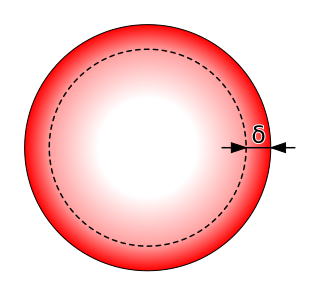
In electromagnetism, skin effect is the tendency of an alternating electric current (AC) to become distributed within a conductor such that the current density is largest near the surface of the conductor and decreases exponentially with greater depths in the conductor. The electric current flows mainly at the "skin" of the conductor, between the outer surface and a level called the skin depth. Skin depth depends on the frequency of the alternating current; as frequency increases, current flow moves to the surface, resulting in less skin depth. Skin effect reduces the effective cross-section of the conductor and thus increases its effective resistance. It is caused by opposing eddy currents induced by the changing magnetic field resulting from the alternating current. At 60 Hz in copper, skin depth is about 8.5 mm. At high frequencies skin depth becomes much smaller.
The van der Pauw Method is a technique commonly used to measure the resistivity and the Hall coefficient of a sample. Its power lies in its ability to accurately measure the properties of a sample of any arbitrary shape, as long as the sample is approximately two-dimensional, solid, and the electrodes are placed on its perimeter. The van der Pauw method employs a four-point probe placed around the perimeter of the sample, in contrast to the linear four point probe: this allows the van der Pauw method to provide an average resistivity of the sample, whereas a linear array provides the resistivity in the sensing direction. This difference becomes important for anisotropic materials, which can be properly measured using the Montgomery Method, an extension of the van der Pauw Method.
Joule heating, also known as resistive, resistance, or Ohmic heating, is the process by which the passage of an electric current through a conductor produces heat.
The Transfer Length Method or the "Transmission Line Model" is a technique used in semiconductor physics and engineering to determine the specific contact resistivity between a metal and a semiconductor. TLM has been developed because with the ongoing device shrinkage in microelectronics the relative contribution of the contact resistance at metal-semiconductor interfaces in a device could not be neglected any more and an accurate measurement method for determining the specific contact resistivity was required.
The piezoresistive effect is a change in the electrical resistivity of a semiconductor or metal when mechanical strain is applied. In contrast to the piezoelectric effect, the piezoresistive effect causes a change only in electrical resistance, not in electric potential.
In electromagnetism, current density is the amount of charge per unit time that flows through a unit area of a chosen cross section. The current density vector is defined as a vector whose magnitude is the electric current per cross-sectional area at a given point in space, its direction being that of the motion of the positive charges at this point. In SI base units, the electric current density is measured in amperes per square metre.
The term contact resistance refers to the contribution to the total resistance of a system which can be attributed to the contacting interfaces of electrical leads and connections as opposed to the intrinsic resistance. This effect is described by the term electrical contact resistance (ECR) and arises as the result of the limited areas of true contact at an interface and the presence of resistive surface films or oxide layers. ECR may vary with time, most often decreasing, in a process known as resistance creep. The idea of potential drop on the injection electrode was introduced by William Shockley to explain the difference between the experimental results and the model of gradual channel approximation. In addition to the term ECR, interface resistance, transitional resistance, or just simply correction term are also used. The term parasitic resistance is used as a more general term, of which it is usually assumed that contact resistance is a major component.
Spreading resistance profiling (SRP), also known as spreading resistance analysis (SRA), is a technique used to analyze resistivity versus depth in semiconductors. Semiconductor devices depend on the distribution of carriers within their structures to provide the desired performance. The carrier concentration can be inferred from the resistivity profile provided by SRP.
Miniaturizing components has always been a primary goal in the semiconductor industry because it cuts production cost and lets companies build smaller computers and other devices. Miniaturization, however, has increased dissipated power per unit area and made it a key limiting factor in integrated circuit performance. Temperature increase becomes relevant for relatively small-cross-sections wires, where it may affect normal semiconductor behavior. Besides, since the generation of heat is proportional to the frequency of operation for switching circuits, fast computers have larger heat generation than slow ones, an undesired effect for chips manufacturers. This article summaries physical concepts that describe the generation and conduction of heat in an integrated circuit, and presents numerical methods that model heat transfer from a macroscopic point of view.
An electric dipole transition is the dominant effect of an interaction of an electron in an atom with the electromagnetic field.
Concrete electrical resistivity can be obtained by applying a current into the concrete and measuring the response voltage. There are different methods for measuring concrete resistivity.

In fluid dynamics, the radiation stress is the depth-integrated – and thereafter phase-averaged – excess momentum flux caused by the presence of the surface gravity waves, which is exerted on the mean flow. The radiation stresses behave as a second-order tensor.
Soil resistivity is a measure of how much the soil resists or conducts electric current. It is a critical factor in design of systems that rely on passing current through the Earth's surface. It is a very important parameter for finding the best location of a transmitter working on low frequiencies as such radio stations usually use ground as counterpole. An understanding of the soil resistivity and how it varies with depth in the soil is necessary to design the grounding system in an electrical substation, or for lightning conductors. It is needed for design of grounding (earthing) electrodes for substations and High-voltage direct current transmission systems. It was formerly important in earth-return telegraphy. It can also be a useful measure in agriculture as a proxy measurement for moisture content.
Space cloth is a hypothetical infinite plane of conductive material having a resistance of η ohms per square, where η is the impedance of free space. η ≈ 376.7 ohms. If a transmission line composed of straight parallel perfect conductors in free space is terminated by space cloth that is normal to the transmission line then that transmission line is terminated by its characteristic impedance. The calculation of the characteristic impedance of a transmission line composed of straight, parallel good conductors may be replaced by the calculation of the D.C. resistance between electrodes placed on a two-dimensional resistive surface. This equivalence can be used in reverse to calculate the resistance between two conductors on a resistive sheet if the arrangement of the conductors is the same as the cross section of a transmission line of known impedance. For example, a pad surrounded by a guard ring on a printed circuit board (PCB) is similar to the cross section of a coaxial cable transmission line.