High-temperature operating life

Last updated

High-temperature operating life (HTOL) is a reliability test applied to integrated circuits (ICs) to determine their intrinsic reliability. This test stresses the IC at an elevated temperature, high voltage and dynamic operation for a predefined period of time. The IC is usually monitored under stress and tested at intermediate intervals. This reliability stress test is sometimes referred to as a lifetime test, device life test or extended burn in test and is used to trigger potential failure modes and assess IC lifetime.

Contents

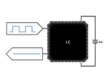
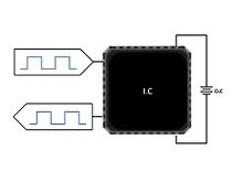
There are several types of HTOL:

HTOL TypesSchematicDescription
Static
Static .jpg
IC stressed at static and constant conditions, IC not toggling.
Dynamic
Dynamic.jpg
Input stimulus for toggling the internal nodes of the device.
Monitored
Monitored.jpg
Input stimulus for toggling the internal nodes of the device. Live output indicates IC performance.
In-situ tested
Tested.jpg
Input stimulus for toggling the internal nodes of the device. Responsive output tests IC performance.

Design considerations

The main aim of the HTOL is to age the device such that a short experiment will allow the lifetime of the IC to be predicted (e.g. 1,000 HTOL hours shall predict a minimum of "X" years of operation). Good HTOL process shall avoid relaxed HTOL operation and also prevents overstressing the IC. This method ages all IC's building blocks to allow relevant failure modes to be triggered and implemented in a short reliability experiment. A precise multiplier, known as the Acceleration Factor (AF) simulates long lifetime operation.

The AF represents the accelerated aging factor relative to the useful life application conditions.

For effective HTOL stress testing, several variables should be considered:

  1. Digital toggling factor
  2. Analog modules operation
  3. I/O ring activity
  4. Monitor design
  5. Ambient temperature (Ta)
  6. Junction temperature (Tj)
  7. Voltage stress (Vstrs)
  8. Acceleration factor (AF)
  9. Test duration (t)
  10. Sample size (SS)

A detailed description of the above variables, using a hypothetical, simplified IC with several RAMs, digital logic, an analog voltage regulator module and I/O ring, together with the HTOL design considerations for each are provided below.

Digital toggling factor

The digital toggling factor (DTF) represents the number of transistors that change their state during the stress test, relative to the total number of gates in the digital portion of the IC. In effect, the DTF is the percentage of transistors toggling in one time unit. The time unit is relative to the toggling frequency, and is usually limited by the HTOL setup to be in the range of 10–20Mhz.

Reliability engineers strive to toggle as many as possible transistors for each time unit of measure. The RAMs (and other memory types) are usually activated using the BIST function, while the logic is usually activated with the SCAN function, LFSR or logic BIST.

The power and the self-heating of the digital portion of the IC are evaluated and the device's aging estimated. These two measures are aligned so that they are similar to the aging of other elements of the IC. The degrees of freedom for aligning these measures are the voltage stress and/or the time period during which the HTOL program loops these blocks relative to other IC blocks.

Analog modules operation

The recent trend of integrating as many electronic components as possible into a single chip is known as system on a chip (SoC).

This trend complicates reliability engineers' work because (usually) the analog portion of the chip dissipates higher power relative to the other IC elements.

This higher power may generate hot spots and areas of accelerated aging. Reliability engineers must understand the power distribution on the chip and align the aging so that it is similar for all elements of an IC.

In our hypothetical SoC the analog module only includes a voltage regulator. In reality, there may be additional analog modules e.g. PMIC, oscillators, or charge pumps. To perform efficient stress tests on the analog elements, reliability engineers must identify the worst-case scenario for the relevant analog blocks in the IC. For example, the worst-case scenario for voltage regulators may be the maximum regulation voltage and maximum load current; for charge pumps it may be the minimum supply voltage and maximum load current.

Good engineering practice calls for the use of external loads (external R,L,C) to force the necessary currents. This practice avoids loading differences due to the chip's different operational schemes and operation trimming of its analog parts.

Statistical methods are used to check statistical tolerances, variation and temperature stability of the loads used, and to define the right confidence bands for the loads to avoid over/under stress at HTOL operating range. The degrees of freedom for aligning the aging magnitude of analog parts is usually the duty-cycle, external load values and voltage stress.

I/O ring activity

The interface between the "outside world" and the IC is made via the input/output (I/O) ring. This ring contains power I/O ports, digital I/O ports and analog I/O ports. The I/Os are (usually) wired via the IC package to the "outside world" and each I/O executes its own specific command instructions, e.g. JTAG ports, IC power supply ports etc. Reliability engineering aims to age all I/Os in the same way as the other IC elements. This can be achieved by using a Boundary scan operation.

Monitor design

As previously mentioned, the main aim of the HTOL is aging the samples by dynamic stress at elevated voltage and/or temperature. During the HTOL operation, we need to assure that the IC is active, toggling and constantly functioning.

At the same time, we need to know at what point the IC stops responding, these data are important for calculating price reliability indices and for facilitating the FA. This is done by monitoring the device via one or more vital IC parameters signals communicated and logged by the HTOL machine and providing continuous indication about the IC's functionality throughout the HTOL run time. Examples of commonly used monitors include the BIST "done" flag signal, the SCAN output chain or the analog module output.

There are three types of monitoring:

  1. Pattern matching: The actual output signal is compared to the expected one and alerts about any deviation. The main disadvantage of this monitor type is its sensitivity to any minor deviation from the expected signal. During the HTOL, the IC runs at a temperature and/or voltages that occasionally fall outside its specification, which may cause artificial sensitivity and/or a malfunction that fails the matching but is not a real failure.
  2. Activity: Counts the number of toggles and if the results are higher than a predefined threshold the monitor indicates OK. The main disadvantage of this type of monitoring is the chance that unexpected noise or signal could be wrongly interpreted. This issue arises mainly in the case of low count toggling monitor.
  3. Activity within a predefine range: Checks that the monitor responds within a predefined limit, for example when then number of toggles is within a predefined limit or the output of the voltage regulator is within a predefined range.

Ambient temperature (Ta)

According to JEDEC standards, the environmental chamber should be capable of maintaining the specified temperature within a tolerance of ±5 °C throughout while parts are loaded and unpowered. Today's environmental chambers have better capabilities and can exhibit temperature stability within a range of ±3 °C throughout.

Junction temperature (Tj)

Low power ICs can be stressed without major attention to self-heating effects. However, due to technology scaling and manufacturing variations, power dissipation within a single production lot of devices can vary by as much as 40%. This variation, in addition to high power IC makes advanced contact temperature controls necessary for facilitating individual control systems for each IC

Voltage stress (Vstrs)

The operating voltage should be at least the maximum specified for the device. In some cases a higher voltage is applied to obtain lifetime acceleration from voltage as well as temperature.

To define the maximum permitted voltage stress, the following methods can be considered:

  1. Force 80% of breakdown voltage;
  2. Force six-sigma less than the breakdown voltage;
  3. Set the overvoltage to be higher than the maximum specified voltage. An overvoltage level of 140% of the maximum voltage is occasionally used for MIL and automotive applications.

Reliability engineers must check that Vstress does not exceed the maximum rated voltage for the relevant technology, as specified by the FAB.

Acceleration factor (AF)

The Acceleration factor (AF) is a multiplier that relates a product's life at an accelerated stress level to the life at the use stress level.

An AF of 20 means 1 hour at stress condition is equivalent to 20 hours at useful condition.

The voltage acceleration factor is represented by AFv. Usually the stress voltage is equal to or higher than the maximum voltage. An elevated voltage provides additional acceleration and can be used to increase effective device hours or achieve an equivalent life point.

There are several AFv models:

  1. E model or the constant field/voltage acceleration exponential model;
  2. 1/E model or, equivalently, the anode hole injection model;
  3. V model, where the failure rate is exponential to voltage
  4. Anode hydrogen release for the power-law model

AFtemp is the acceleration factor due to changes in temperature and is usually based on the Arrhenius equation. The total acceleration factor is the product of AFv and AFtemp

Test duration (t)

The reliability test duration assures the device's adequate lifetime requirement.

For example, with an activation energy of 0.7 eV, 125 °C stress temperature and 55 °C use temperature, the acceleration factor (Arrhenius equation) is 78.6. This means that 1,000 hours' stress duration is equivalent to 9 years of use. The reliability engineer decides on the qualification test duration. Industry good practice calls for 1,000 hours at a junction temperature of 125 °C.

Sample size (SS)

The challenge for new reliability assessment and qualification systems is determining the relevant failure mechanisms to optimize sample size.

Sample plans are statistically derived from manufacturer risk, consumer risk, and the expected failure rate. The commonly used sampling plan of zero rejects out of 230 samples is equal to three rejects out of 668 samples assuming LTPD =1 and a 90% confidence interval.

HTOL policy

Sample selection

Samples shall include representative samples from at least three nonconsecutive lots to represent manufacturing variability. All test samples shall be fabricated, handled, screened and assembled in the same way as during the production phase.

Sample preparation

Samples shall be tested prior to stress and at predefined checkpoints. It is good engineering practice to test samples at maximum and minimum rating temperatures as well as at room temperature. Data logs of all functional and parametric tests shall be collated for further analysis.

Test duration

Assuming Tj = 125 °C, commonly used checkpoints are after 48, 168, 500 and 1,000 hours.

Different checkpoints for different temperatures can be calculated by using the Arrhenius equation. For example, with an activation energy of 0.7e V, Tj of 135 °C and Tuse of 55 °C the equivalent checkpoints will be at 29, 102, 303 and 606 hours.

Electrical testing should be completed as soon as possible after the samples are removed. If the samples cannot be tested soon after their removal, additional stress time should be applied. The JEDEC standard requires samples be tested within 168 hours of removal.

If testing exceeds the recommended time window, additional stress should be applied according to the table below: [2]

Time above recommended time window0h < h ≤ 168h168h < h ≤ 336h336h < h ≤ 504hOther
Additional stress hours24h48h72h24 hours for each 168 hours

Merit numbers

The merit number is the outcome of statistical sampling plans.

Sampling plans are inputted to SENTENCE, an audit tool, to ensure that the output of a process meets the requirements. SENTENCE simply accepts or rejects the tested lots. The reliability engineer implements statistical sampling plans based on predefined Acceptance Quality Limits, LTPD, manufacturer risk and customer risk. For example, the commonly used sampling plan of 0 rejects out of 230 samples is equal to 3 rejects out of 668 samples assuming LTPD=1.

HTOL in various industries

The aging process of an IC is relative to its standard use conditions. The tables below provide reference to various commonly used products and the conditions under which they are used.

Reliability engineers are tasked with verifying the adequate stress duration. For example, for an activation energy of 0.7eV, a stress temperature of 125 °C and a use temperature of 55 °C, an expected operational life of five years is represented by a 557-hour HTOL experiment.

Commercial use

Min TuseMax TuseDescriptionExpected life time
5 °C50 °Cdesktop products5 years
0 °C70 °Cmobile products4 years

Automotive use

Example Automotive Use Conditions [1]

Min TuseMax TuseDescriptionExpected life time
−40 °C105—150 °Cunder hood condition10 to 15 years
−40 °C80 °Cpassenger compartment condition10 to 15 years
0 °C70 °Cpassenger compartment condition10 to 15 years

Telecommunication use

Example European Telecom use Conditions definition

Min TuseMax TuseDescriptionExpected life time
5 °C40 °Cclass 3.1 Temperature-controlled locationsusually 25 years
−5 °C45 °Cclass 3.2 Partly temperature-controlled locationsusually 25 years
−25 °C55 °Cclass 3.3 Not temperature-controlled locationsusually 25 years
−40 °C70 °Cclass 3.4 Sites with heat-trapusually 25 years
−40 °C40 °Cclass 3.5 Sheltered locations, Direct solar radiationusually 25 years

Example US Telecom use conditions definition

Min TuseMax TuseDescriptionExpected life time
−40 °C46 °CUncontrolled environment25 years
5 °C40 °CEnclosed building25 years

Military use

Example military use conditions

Min TuseMax TuseDescription
−55 °C125 °CMIL products
−55 °Cup to 225 °Chigh-temp applications

Example

Number of Failures = r

Number of Devices = D

Test Hours per Device = H

Celsius + 273 = T (Calculation Temperature in Kelvin)

Test Temperature (HTRB or other burn-in temperature)=

Use Temperature (standardized at 55 °C or 328K) =

Activation Energy (eV) =

Chi Squared/2 is the probability estimation for number of failures at α and ν

Confidence Level for X^2 distribution; reliability calculations use α=60% or .60 = α (alpha)
Degrees of Freedom for distribution; reliability calculations use ν=2r + 2. = ν (nu)

Acceleration Factor from the Arrhenius equation =

Boltzmann's Constant ( ) = 8.617 x 10e-5 eV/K

Device Hours (DH) = D x H

Equivalent Device Hours (EDH) = D x H x

Failure Rate per hour =

Failures in Time = Failure Rate per billion hours = FIT =

Mean Time to Failure = MTTF

Where the Acceleration Factor from the Arrhenius equation is:

Failure Rate per hour =

Failures in Time = Failure Rate per billion hours = FIT =

Mean Time to Failure in hours =

Mean Time to Failure in years= ´

In case you want to calculate the acceleration factor including the Humidity the so-called Highly accelerated stress test (HAST), then:

the Acceleration Factor from the Arrhenius equation would be:

where is the stress test relative humidity (in percentage). Typically is 85%.

where is the typical use relative humidity (in percentage). Typically this is measured at the chip surface ca. 10–20%.

where is the failure mechanism scale factor. Which is a value between 0.1 and 0.15.

In case you want to calculate the acceleration factor including the Humidity (HAST) and voltage stress then:

the Acceleration Factor from the Arrhenius equation would be:

where is the stress voltage (in volts). Typically is the VCCx1.4 volts. e.g. 1.8x1.4=2.52 volts.

where is the typical usage voltage or VCC (in volts). Typically VCC is 1.8v. Depending on the design.

where is the failure mechanism scale factor. Which is a value between 0 and 3.0. Typically 0.5 for Silican junction defect.

See also

Related Research Articles

<span class="mw-page-title-main">Exponential distribution</span> Probability distribution

In probability theory and statistics, the exponential distribution or negative exponential distribution is the probability distribution of the distance between events in a Poisson point process, i.e., a process in which events occur continuously and independently at a constant average rate; the distance parameter could be any meaningful mono-dimensional measure of the process, such as time between production errors, or length along a roll of fabric in the weaving manufacturing process. It is a particular case of the gamma distribution. It is the continuous analogue of the geometric distribution, and it has the key property of being memoryless. In addition to being used for the analysis of Poisson point processes it is found in various other contexts.

Mean time between failures (MTBF) is the predicted elapsed time between inherent failures of a mechanical or electronic system during normal system operation. MTBF can be calculated as the arithmetic mean (average) time between failures of a system. The term is used for repairable systems while mean time to failure (MTTF) denotes the expected time to failure for a non-repairable system.

Survival analysis is a branch of statistics for analyzing the expected duration of time until one event occurs, such as death in biological organisms and failure in mechanical systems. This topic is called reliability theory or reliability analysis in engineering, duration analysis or duration modelling in economics, and event history analysis in sociology. Survival analysis attempts to answer certain questions, such as what is the proportion of a population which will survive past a certain time? Of those that survive, at what rate will they die or fail? Can multiple causes of death or failure be taken into account? How do particular circumstances or characteristics increase or decrease the probability of survival?

A current mirror is a circuit designed to copy a current through one active device by controlling the current in another active device of a circuit, keeping the output current constant regardless of loading. The current being "copied" can be, and sometimes is, a varying signal current. Conceptually, an ideal current mirror is simply an ideal inverting current amplifier that reverses the current direction as well, or it could consist of a current-controlled current source (CCCS). The current mirror is used to provide bias currents and active loads to circuits. It can also be used to model a more realistic current source.

<span class="mw-page-title-main">Electromigration</span> Movement of ions in an electrical field

Electromigration is the transport of material caused by the gradual movement of the ions in a conductor due to the momentum transfer between conducting electrons and diffusing metal atoms. The effect is important in applications where high direct current densities are used, such as in microelectronics and related structures. As the structure size in electronics such as integrated circuits (ICs) decreases, the practical significance of this effect increases.

<span class="mw-page-title-main">Thomson scattering</span> Low energy photon scattering off charged particles

Thomson scattering is the elastic scattering of electromagnetic radiation by a free charged particle, as described by classical electromagnetism. It is the low-energy limit of Compton scattering: the particle's kinetic energy and photon frequency do not change as a result of the scattering. This limit is valid as long as the photon energy is much smaller than the mass energy of the particle: , or equivalently, if the wavelength of the light is much greater than the Compton wavelength of the particle.

Failure rate is the frequency with which an engineered system or component fails, expressed in failures per unit of time. It is usually denoted by the Greek letter λ (lambda) and is often used in reliability engineering.

In probability theory and statistics, the noncentral F-distribution is a continuous probability distribution that is a noncentral generalization of the (ordinary) F-distribution. It describes the distribution of the quotient (X/n1)/(Y/n2), where the numerator X has a noncentral chi-squared distribution with n1 degrees of freedom and the denominator Y has a central chi-squared distribution with n2 degrees of freedom. It is also required that X and Y are statistically independent of each other.

Thermal shock is a phenomenon characterized by a rapid change in temperature that results in a transient mechanical load on an object. The load is caused by the differential expansion of different parts of the object due to the temperature change. This differential expansion can be understood in terms of strain, rather than stress. When the strain exceeds the tensile strength of the material, it can cause cracks to form and eventually lead to structural failure.

Optical resolution describes the ability of an imaging system to resolve detail, in the object that is being imaged. An imaging system may have many individual components, including one or more lenses, and/or recording and display components. Each of these contributes to the optical resolution of the system; the environment in which the imaging is done often is a further important factor.

In general relativity, a geodesic generalizes the notion of a "straight line" to curved spacetime. Importantly, the world line of a particle free from all external, non-gravitational forces is a particular type of geodesic. In other words, a freely moving or falling particle always moves along a geodesic.

<span class="mw-page-title-main">Channel length modulation</span> Effect in field effect transistors

Channel length modulation (CLM) is an effect in field effect transistors, a shortening of the length of the inverted channel region with increase in drain bias for large drain biases. The result of CLM is an increase in current with drain bias and a reduction of output resistance. It is one of several short-channel effects in MOSFET scaling. It also causes distortion in JFET amplifiers.

Rubber elasticity refers to a property of crosslinked rubber: it can be stretched by up to a factor of 10 from its original length and, when released, returns very nearly to its original length. This can be repeated many times with no apparent degradation to the rubber. Rubber is a member of a larger class of materials called elastomers and it is difficult to overestimate their economic and technological importance. Elastomers have played a key role in the development of new technologies in the 20th century and make a substantial contribution to the global economy. Rubber elasticity is produced by several complex molecular processes and its explanation requires a knowledge of advanced mathematics, chemistry and statistical physics, particularly the concept of entropy. Entropy may be thought of as a measure of the thermal energy that is stored in a molecule. Common rubbers, such as polybutadiene and polyisoprene, are produced by a process called polymerization. Very long molecules (polymers) are built up sequentially by adding short molecular backbone units through chemical reactions. A rubber polymer follows a random, zigzag path in three dimensions, intermingling with many other rubber molecules. An elastomer is created by the addition of a few percent of a cross linking molecule such as sulfur. When heated, the crosslinking molecule causes a reaction that chemically joins (bonds) two of the rubber molecules together at some point. Because the rubber molecules are so long, each one participates in many crosslinks with many other rubber molecules forming a continuous molecular network. As a rubber band is stretched, some of the network chains are forced to become straight and this causes a decrease in their entropy. It is this decrease in entropy that gives rise to the elastic force in the network chains.

The Weibull modulus is a dimensionless parameter of the Weibull distribution which is used to describe variability in measured material strength of brittle materials.

The linear attenuation coefficient, attenuation coefficient, or narrow-beam attenuation coefficient characterizes how easily a volume of material can be penetrated by a beam of light, sound, particles, or other energy or matter. A coefficient value that is large represents a beam becoming 'attenuated' as it passes through a given medium, while a small value represents that the medium had little effect on loss. The (derived) SI unit of attenuation coefficient is the reciprocal metre (m−1). Extinction coefficient is another term for this quantity, often used in meteorology and climatology. Most commonly, the quantity measures the exponential decay of intensity, that is, the value of downward e-folding distance of the original intensity as the energy of the intensity passes through a unit thickness of material, so that an attenuation coefficient of 1 m−1 means that after passing through 1 metre, the radiation will be reduced by a factor of e, and for material with a coefficient of 2 m−1, it will be reduced twice by e, or e2. Other measures may use a different factor than e, such as the decadic attenuation coefficient below. The broad-beam attenuation coefficient counts forward-scattered radiation as transmitted rather than attenuated, and is more applicable to radiation shielding. The mass attenuation coefficient is the attenuation coefficient normalized by the density of the material.

<span class="mw-page-title-main">Conway–Maxwell–Poisson distribution</span> Probability distribution

In probability theory and statistics, the Conway–Maxwell–Poisson distribution is a discrete probability distribution named after Richard W. Conway, William L. Maxwell, and Siméon Denis Poisson that generalizes the Poisson distribution by adding a parameter to model overdispersion and underdispersion. It is a member of the exponential family, has the Poisson distribution and geometric distribution as special cases and the Bernoulli distribution as a limiting case.

<span class="mw-page-title-main">Poisson distribution</span> Discrete probability distribution

In probability theory and statistics, the Poisson distribution is a discrete probability distribution that expresses the probability of a given number of events occurring in a fixed interval of time if these events occur with a known constant mean rate and independently of the time since the last event. It can also be used for the number of events in other types of intervals than time, and in dimension greater than 1.

The wafer bond characterization is based on different methods and tests. Considered a high importance of the wafer are the successful bonded wafers without flaws. Those flaws can be caused by void formation in the interface due to unevenness or impurities. The bond connection is characterized for wafer bond development or quality assessment of fabricated wafers and sensors.

Software reliability testing is a field of software-testing that relates to testing a software's ability to function, given environmental conditions, for a particular amount of time. Software reliability testing helps discover many problems in the software design and functionality.

In mathematics and physics, acceleration is the rate of change of velocity of a curve with respect to a given linear connection. This operation provides us with a measure of the rate and direction of the "bend".

References