Physical design (electronics)

Last updated

In integrated circuit design, physical design is a step in the standard design cycle which follows after the circuit design. At this step, circuit representations of the components (devices and interconnects) of the design are converted into geometric representations of shapes which, when manufactured in the corresponding layers of materials, will ensure the required functioning of the components. This geometric representation is called integrated circuit layout. This step is usually split into several sub-steps, which include both design and verification and validation of the layout. [1] [2]

Contents

Modern day Integrated Circuit (IC) design is split up into Front-end Design using HDLs and Back-end Design or Physical Design. The inputs to physical design are (i) a netlist, (ii) library information on the basic devices in the design, and (iii) a technology file containing the manufacturing constraints. Physical design is usually concluded by Layout Post Processing, in which amendments and additions to the chip layout are performed. [3] This is followed by the Fabrication or Manufacturing Process where designs are transferred onto silicon dies which are then packaged into ICs.

Each of the phases mentioned above has design flows associated with them. These design flows lay down the process and guide-lines/framework for that phase. The physical design flow uses the technology libraries that are provided by the fabrication houses. These technology files provide information regarding the type of silicon wafer used, the standard-cells used, the layout rules (like DRC in VLSI), etc.

Physical design steps within the IC design flow PhysicalDesign.png
Physical design steps within the IC design flow

Divisions

Typically, the IC physical design is categorized into full custom and semi-custom design.

One can use ASIC for Full Custom design and FPGA for Semi-Custom design flows. The reason being that one has the flexibility to design/modify design blocks from vendor provided libraries in ASIC. [5] This flexibility is missing for Semi-Custom flows using FPGAs (e.g. Altera).

ASIC physical design flow

A typical ASIC back-end flow PD Flow.gif
A typical ASIC back-end flow

The main steps in the ASIC physical design flow are:

These steps are just the basics. There are detailed PD flows that are used depending on the Tools used and the methodology/technology. Some of the tools/software used in the back-end design are:

The ASIC physical design flow uses the technology libraries that are provided by the fabrication houses. Technologies are commonly classified according to minimal feature size. Standard sizes, in the order of miniaturization, are 2μm, 1μm , 0.5μm , 0.35μm, 0.25μm, 180nm, 130nm, 90nm, 65nm, 45nm, 28nm, 22nm, 18nm, 14nm, etc. They may be also classified according to major manufacturing approaches: n-Well process, twin-well process, SOI process, etc.

Design netlist

Physical design is based on a netlist which is the end result of the synthesis process. Synthesis converts the RTL design usually coded in VHDL or Verilog HDL to gate-level descriptions which the next set of tools can read/understand. This netlist contains information on the cells used, their interconnections, area used, and other details. Typical synthesis tools are:

During the synthesis process, constraints are applied to ensure that the design meets the required functionality and speed (specifications). Only after the netlist is verified for functionality and timing it is sent for the physical design flow.

Steps

Partitioning

Partitioning is a process of dividing the chip into small blocks. This is done mainly to separate different functional blocks and also to make placement and routing easier. Partitioning can be done in the RTL design phase when the design engineer partitions the entire design into sub-blocks and then proceeds to design each module. These modules are linked together in the main module called the TOP LEVEL module. This kind of partitioning is commonly referred to as Logical Partitioning. The goal of partitioning is to split the circuit such that the number of connections between partitions is minimized.


Floorplanning

The second step in the physical design flow is floorplanning . Floorplanning is the process of identifying structures that should be placed close together, and allocating space for them in such a manner as to meet the sometimes conflicting goals of available space (cost of the chip), required performance, and the desire to have everything close to everything else.

Based on the area of the design and the hierarchy, a suitable floorplan is decided upon. Floorplanning takes into account the macros used in the design, memory, other IP cores and their placement needs, the routing possibilities, and also the area of the entire design. Floorplanning also determines the IO structure and aspect ratio of the design. A bad floorplan will lead to wastage of die area and routing congestion.

In many design methodologies, area and speed are the subjects of trade-offs. This is due to limited routing resources, as the more resources used, the slower the operation. Optimizing for minimum area allows the design both to use fewer resources, and for greater proximity of the sections of the design. This leads to shorter interconnect distances, fewer routing resources used, faster end-to-end signal paths, and even faster and more consistent place and route times. Done correctly, there are no negatives to floorplanning.

As a general rule, data-path sections benefit most from floorplanning, whereas random logic, state machines, and other non-structured logic can safely be left to the placer section of the place and route software.

Data paths are typically the areas of the design where multiple bits are processed in parallel with each bit being modified the same way with maybe some influence from adjacent bits. Example structures that make up data paths are Adders, Subtractors, Counters, Registers, and Muxes.


Placement

Before the start of placement optimization all Wire Load Models (WLM) are removed. Placement uses RC values from Virtual Route (VR) to calculate timing. VR is the shortest Manhattan distance between two pins. VR RCs are more accurate than WLM RCs.

Placement is performed in four optimization phases:

  1. Pre-placement optimization
  2. In placement optimization
  3. Post Placement Optimization (PPO) before clock tree synthesis (CTS)
  4. PPO after CTS.

Clock tree synthesis

Ideal clock before CTS Ideal clock.png
Ideal clock before CTS

The goal of clock tree synthesis (CTS) is to minimize skew and insertion delay. Clock is not propagated before CTS as shown in the picture. After CTS hold slack should improve. Clock tree begins at .sdc defined clock source and ends at stop pins of flop. There are two types of stop pins known as ignore pins and sync pins. 'Don't touch' circuits and pins in front end (logic synthesis) are treated as 'ignore' circuits or pins at back end (physical synthesis). 'Ignore' pins are ignored for timing analysis. If clock is divided then separate skew analysis is necessary.

Rigidity is the term coined in Astro to indicate the relaxation of constraints. Higher the rigidity tighter is the constraints.

Clock After CTS Clock after CTS.PNG
Clock After CTS

In clock tree optimization (CTO) clock can be shielded so that noise is not coupled to other signals. But shielding increases area by 12 to 15%. Since the clock signal is global in nature the same metal layer used for power routing is used for clock also. CTO is achieved by buffer sizing, gate sizing, buffer relocation, level adjustment and HFN synthesis. We try to improve setup slack in pre-placement, in placement and post placement optimization before CTS stages while neglecting hold slack. In post placement optimization after CTS hold slack is improved. As a result of CTS lot of buffers are added. Generally for 100k gates around 650 buffers are added.

Routing

There are two types of routing in the physical design process, global routing and detailed routing. Global routing allocates routing resources that are used for connections. It also does track assignment for a particular net.

Detailed routing does the actual connections. Different constraints that are to be taken care during the routing are DRC, wire length, timing etc.

Physical verification

Physical verification checks the correctness of the generated layout design. This includes verifying that the layout

Layout post processing

Layout Post Processing, also known mask data preparation, often concludes physical design and verification. It converts the physical layout (polygons) into mask data (instructions for the photomask writer). It includes [3]

See also

Related Research Articles

In computer engineering, a hardware description language (HDL) is a specialized computer language used to describe the structure and behavior of electronic circuits, most commonly to design ASICs and program FPGAs.

<span class="mw-page-title-main">Application-specific integrated circuit</span> Integrated circuit customized for a specific task

An application-specific integrated circuit is an integrated circuit (IC) chip customized for a particular use, rather than intended for general-purpose use, such as a chip designed to run in a digital voice recorder or a high-efficiency video codec. Application-specific standard product chips are intermediate between ASICs and industry standard integrated circuits like the 7400 series or the 4000 series. ASIC chips are typically fabricated using metal–oxide–semiconductor (MOS) technology, as MOS integrated circuit chips.

Electronic design automation (EDA), also referred to as electronic computer-aided design (ECAD), is a category of software tools for designing electronic systems such as integrated circuits and printed circuit boards. The tools work together in a design flow that chip designers use to design and analyze entire semiconductor chips. Since a modern semiconductor chip can have billions of components, EDA tools are essential for their design; this article in particular describes EDA specifically with respect to integrated circuits (ICs).

In digital circuit design, register-transfer level (RTL) is a design abstraction which models a synchronous digital circuit in terms of the flow of digital signals (data) between hardware registers, and the logical operations performed on those signals.

Formal equivalence checking process is a part of electronic design automation (EDA), commonly used during the development of digital integrated circuits, to formally prove that two representations of a circuit design exhibit exactly the same behavior.

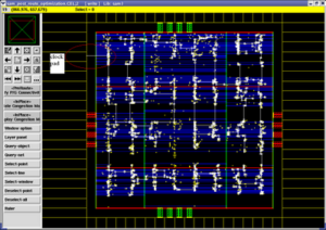
Place and route is a stage in the design of printed circuit boards, integrated circuits, and field-programmable gate arrays. As implied by the name, it is composed of two steps, placement and routing. The first step, placement, involves deciding where to place all electronic components, circuitry, and logic elements in a generally limited amount of space. This is followed by routing, which decides the exact design of all the wires needed to connect the placed components. This step must implement all the desired connections while following the rules and limitations of the manufacturing process.

VLSI Technology, Inc., was an American company that designed and manufactured custom and semi-custom integrated circuits (ICs). The company was based in Silicon Valley, with headquarters at 1109 McKay Drive in San Jose. Along with LSI Logic, VLSI Technology defined the leading edge of the application-specific integrated circuit (ASIC) business, which accelerated the push of powerful embedded systems into affordable products.

In electronic design, a semiconductor intellectual property core, IP core or IP block is a reusable unit of logic, cell, or integrated circuit layout design that is the intellectual property of one party. IP cores can be licensed to another party or owned and used by a single party. The term comes from the licensing of the patent or source code copyright that exists in the design. Designers of system on chip (SoC), application-specific integrated circuits (ASIC) and systems of field-programmable gate array (FPGA) logic can use IP cores as building blocks.

<span class="mw-page-title-main">Standard cell</span>

In semiconductor design, standard-cell methodology is a method of designing application-specific integrated circuits (ASICs) with mostly digital-logic features. Standard-cell methodology is an example of design abstraction, whereby a low-level very-large-scale integration (VLSI) layout is encapsulated into an abstract logic representation.

<span class="mw-page-title-main">Integrated circuit design</span> Engineering process for electronic hardware

Integrated circuit design, or IC design, is a sub-field of electronics engineering, encompassing the particular logic and circuit design techniques required to design integrated circuits, or ICs. ICs consist of miniaturized electronic components built into an electrical network on a monolithic semiconductor substrate by photolithography.

Placement is an essential step in electronic design automation — the portion of the physical design flow that assigns exact locations for various circuit components within the chip's core area. An inferior placement assignment will not only affect the chip's performance but might also make it non-manufacturable by producing excessive wire-length, which is beyond available routing resources. Consequently, a placer must perform the assignment while optimizing a number of objectives to ensure that a circuit meets its performance demands. Together, the placement and routing steps of IC design are known as place and route.

Design flows are the explicit combination of electronic design automation tools to accomplish the design of an integrated circuit. Moore's law has driven the entire IC implementation RTL to GDSII design flows from one which uses primarily stand-alone synthesis, placement, and routing algorithms to an integrated construction and analysis flows for design closure. The challenges of rising interconnect delay led to a new way of thinking about and integrating design closure tools.

An EDA database is a database specialized for the purpose of electronic design automation. These application specific databases are required because general purpose databases have historically not provided enough performance for EDA applications.

Physical verification is a process whereby an integrated circuit layout design is verified via EDA software tools to ensure correct electrical and logical functionality and manufacturability. Verification involves design rule check (DRC), layout versus schematic (LVS), XOR, antenna checks and electrical rule check (ERC).

Design Closure is a part of the digital electronic design automation workflow by which an integrated circuit design is modified from its initial description to meet a growing list of design constraints and objectives.

The Timing closure in VLSI design and electronics engineering is the process by which a logic design of a clocked synchronous circuit consisting of primitive elements such as combinatorial logic gates and sequential logic gates is modified to meet its timing requirements. Unlike in a computer program where there is no explicit delay to perform a calculation, logic circuits have intrinsic and well defined delays to propagate inputs to outputs.

<span class="mw-page-title-main">Floorplan (microelectronics)</span> Layout of major electronic circuit blocks

In electronic design automation, a floorplan of an integrated circuit is a schematic representation of tentative placement of its major functional blocks.

Field-programmable gate array prototyping, also referred to as FPGA-based prototyping, ASIC prototyping or system-on-chip (SoC) prototyping, is the method to prototype system-on-chip and application-specific integrated circuit designs on FPGAs for hardware verification and early software development.

Catapult C Synthesis, a commercial electronic design automation product of Mentor Graphics, is a high-level synthesis tool, sometimes called algorithmic synthesis or ESL synthesis. Catapult C takes ANSI C/C++ and SystemC inputs and generates register transfer level (RTL) code targeted to FPGAs and ASICs.

In the automated design of integrated circuits, signoff checks is the collective name given to a series of verification steps that the design must pass before it can be taped out. This implies an iterative process involving incremental fixes across the board using one or more check types, and then retesting the design. There are two types of sign-off's: front-end sign-off and back-end sign-off. After back-end sign-off, the chip goes to fabrication. After listing out all the features in the specification, the verification engineer will write coverage for those features to identify bugs, and send back the RTL design to the designer. Bugs, or defects, can include issues like missing features, errors in design, etc. When the coverage reaches a maximum percentage then the verification team will sign it off. By using a methodology like UVM, OVM, or VMM, the verification team develops a reusable environment. Nowadays, UVM is more popular than others.

References

  1. N. Sherwani, "Algorithms for VLSI Physical Design Automation", Kluwer (1998), ISBN   9780792383932
  2. A. Kahng, J. Lienig, I. Markov, J. Hu: "VLSI Physical Design: From Graph Partitioning to Timing Closure", Springer (2022), doi : 10.1007/978-90-481-9591-6, ISBN   978-3-030-96414-6, pp. 6-10.
  3. 1 2 J. Lienig, J. Scheible (2020). "Chap. 3.3: Mask Data: Layout Post Processing". Fundamentals of Layout Design for Electronic Circuits. Springer. p. 102-110. doi:10.1007/978-3-030-39284-0. ISBN   978-3-030-39284-0. S2CID   215840278.
  4. Semi-Custom Design Flow
  5. Mehrotra, Alok; Van Ginneken, Lukas P P P; Trivedi, Yatin. "Design flow and methodology for 50M gate ASIC", IEEE Conference Publications, ISBN   0-7803-7659-5
  6. A. Kahng, J. Lienig, I. Markov, J. Hu: "VLSI Physical Design: From Graph Partitioning to Timing Closure", Springer (2022), doi : 10.1007/978-3-030-96415-3, ISBN   978-3-030-96414-6, p. 26.