Platinum diselenide

Last updated
Platinum diselenide
Names
Other names
Platinum(IV) selenide
Sudovikovite
Identifiers
3D model (JSmol)
PubChem CID
  • InChI=1S/Pt.2Se Yes check.svgY
    Key: JTPDXCIVXNLRFP-UHFFFAOYSA-N Yes check.svgY
  • [Se]=[Pt]=[Se]
Properties
PtSe2
Molar mass 353.026 g·mol−1
Appearanceopaque metallic yellowish white
Density 9.54
Melting point decomposes
insoluble
Band gap 0 (bulk) 1.3 eV monolayer
Structure
space group P3m1 164 hexagonal
a = 3.728 [1] , c = 5.031
octahedral
Related compounds
Other anions
platinum disulfide platinum ditelluride PtSeTe PtSSe
Other cations
palladium diselenide NiSeTe
Related platinum selenides
Luberoite Pt5Se4
Except where otherwise noted, data are given for materials in their standard state (at 25 °C [77 °F], 100 kPa).
X mark.svgN (what is  Yes check.svgYX mark.svgN ?)

Platinum diselenide is a transition metal dichalcogenide with the formula PtSe2. It is a layered substance that can be split into layers down to three atoms thick. PtSe2 can behave as a metalloid or as a semiconductor depending on the thickness.

Contents

Synthesis

Minozzi was the first to report synthesising platinum diselenide from the elements in 1909. [2]

Platinum diselenide can be formed by heating thin foils of platinum in selenium vapour at 400 °C. [3] [4]

A platinum 111 surface exposed to selenium vapour at 270 °C forms a monolayer of PtSe2. [5]

In addition to these selenization methods, PtSe2 can be made by precipitation in water solution of Pt(IV) treated with hydrogen selenide, or by heating platinum tetrachloride with elemental selenium. [2]

Natural occurrence

Platinum diselenide occurs naturally as the mineral Sudovikovite. It was named after Russian petrologist, N.G. Sudovikov who lived from 1903 to 1966. The mineral's hardness is 2 to 21/2. Sudovikovite was found in the Srednyaya Padma mine, Velikaya Guba uranium-vanadium deposit, Zaonezhie peninsula, Karelia Republic, Russia. [6]

Properties

Platinum diselenide forms crystals in the cadmium iodide structure. This means that the substance forms layers. Each of the monolayers has a central bed of platinum atoms, with a sheet of selenium atoms above and below. This structure is also called "1T" and has an trigonal structure. The layers are only weakly bonded together, and it is possible to exfoliate layers to bilayers or monolayers. [7]

In bulk the material is semi-metallic, but when reduced to few layers it becomes a semiconductor. [7] [8] The conductivity of the bulk material is 620,000 S/m. [9]

The XPS spectrum shows a peak at 72.3 eV from Pt 4f core, and also has peaks from Pt 5p3/2 [7] and Se 3d3/2 and 3d5/2 at 55.19and 54.39 eV. [5]

Phonon vibrations are designated by the infrared active A2u (Se vibrating out of plane opposite to Pt), Eu (in layer vibration, Se opposite to Pt), and Raman active A1g (Se top and bottom atoms moving out of plane in opposite directions 205 cm−1), and Eg (In plane, top and bottom Se atoms moving opposite 175 cm−1). In the Raman spectrum, the A1g is lessened when stimulated emissions polarised perpendicular to the incoming rays are measured. The Eg mode is red-shifted when more layers are stacked. (166 cm−1 for bilayer and 155 cm−1 for bulk material) The A1g emission only has a slight change when thickness varies. [7]

The band gap is calculated as 1.2 eV for monolayers, and 0.21 eV for bilayers. For a trylayer or thicker the substance loses a bandgap and becomes semimetallic. [5]

PtSe2 can change its conductance in the presence of particular gases, such as nitrogen dioxide. Within a few seconds, NO2 absorbs on the surface of the PtSe2 material and lowers the resistance. When the gas is absent, high resistance returns again in about a minute. [3]

The Seebeck coefficient of PtSe2 is 40 μV/K. [10]

Although pristine platinum diselenide is nonmagnetic, the presence of platinum vacancies and strain were predicted to induce magnetism. [11] Later magneto-transport studies [12] have indeed shown that defective PtSe2 exhibits magnetic properties. Due to RKKY interaction between magnetic Pt-vacancies, this results in layer-dependent ferromagnetic or anti-ferromagnetic behavior.

Monolayers of platinum diselenide show helical spin texture, which is not expected for centrosymmetric materials such as this. This property could be due to a local dipole induced Rashba effect. It means that PtSe2 is a potential spintronics material. [13]

Reactions

Water can physisorb to the surface of platinum diselenide with an energy of −0.19 eV, and similarly for oxygen with energy −0.13 eV. Water and oxygen do not react at toom temperature, because significant energy would be required to break apart the molecules. [9]

Comparison

Palladium diselenide has a different modified pyrite structure. Palladium ditelluride has a similar structure to platinum diselenide. [14] Platinum disulfide is a semiconductor, and platinum ditelluride is metallic in nature.

More complex substances with platinum and selenium also exist, including the quaternary chalcogenides Rb2Pt3USe6 and Cs2Pt3USe6 [15]

Jacutingaite is a ternary platinum selenide HgPtSe3. [16]

Use

Platinum diselenide can be utilized for boardband photodetector up to mid-infrared (MIR) region with stability in ambient condition. [17] Also it can work as a catalyst, and can be built into field effect transistors. [9]

Combined with graphene it can be a photocatalyst, converting water and oxygen to reactive hydroxyl radical and superoxide. This reaction works when photons produce holes and electrons. The holes can neutralise hydroxide to make hydroxyl, and the electrons attach to oxygen to make superoxide. These reactive species can mineralise organic matter.

Related Research Articles

A bilayer is a double layer of closely packed atoms or molecules.

<span class="mw-page-title-main">Chalcogenide</span>

A chalcogenide is a chemical compound consisting of at least one chalcogen anion and at least one more electropositive element. Although all group 16 elements of the periodic table are defined as chalcogens, the term chalcogenide is more commonly reserved for sulfides, selenides, tellurides, and polonides, rather than oxides. Many metal ores exist as chalcogenides. Photoconductive chalcogenide glasses are used in xerography. Some pigments and catalysts are also based on chalcogenides. The metal dichalcogenide MoS2 is a common solid lubricant.

<span class="mw-page-title-main">Mercury selenide</span> Chemical compound

Mercury selenide is a chemical compound of mercury and selenium. It is a grey-black crystalline solid semi-metal with a sphalerite structure. The lattice constant is 0.608 nm.

<span class="mw-page-title-main">Tin selenide</span> Chemical compound

Tin selenide, also known as stannous selenide, is an inorganic compound with the formula SnSe. Tin(II) selenide is a typical layered metal chalcogenide as it includes a group 16 anion (Se2−) and an electropositive element (Sn2+), and is arranged in a layered structure. Tin(II) selenide is a narrow band-gap (IV-VI) semiconductor structurally analogous to black phosphorus. It has received considerable interest for applications including low-cost photovoltaics, and memory-switching devices.

<span class="mw-page-title-main">Copper indium gallium selenide solar cell</span>

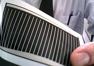
A copper indium gallium selenide solar cell is a thin-film solar cell used to convert sunlight into electric power. It is manufactured by depositing a thin layer of copper indium gallium selenide solid solution on glass or plastic backing, along with electrodes on the front and back to collect current. Because the material has a high absorption coefficient and strongly absorbs sunlight, a much thinner film is required than of other semiconductor materials.

<span class="mw-page-title-main">Sodium selenide</span> Chemical compound

Sodium selenide is an inorganic compound of sodium and selenium with the chemical formula Na2Se.

<span class="mw-page-title-main">Titanium diselenide</span> Chemical compound

Titanium diselenide (TiSe2) also known as titanium(IV) selenide, is an inorganic compound of titanium and selenium. In this material selenium is viewed as selenide (Se2−) which requires that titanium exists as Ti4+. Titanium diselenide is a member of metal dichalcogenides, compounds that consist of a metal and an element of the chalcogen column within the periodic table. Many exhibit properties of potential value in battery technology, such as intercalation and electrical conductivity, although most applications focus on the less toxic and lighter disulfides, e.g. TiS2.

<span class="mw-page-title-main">Molybdenum diselenide</span> Chemical compound

Molybdenum diselenide is an inorganic compound of molybdenum and selenium. Its structure is similar to that of MoS
2
. Compounds of this category are known as transition metal dichalcogenides, abbreviated TMDCs. These compounds, as the name suggests, are made up of a transition metals and elements of group 16 on the periodic table of the elements. Compared to MoS
2
, MoSe
2
exhibits higher electrical conductivity.

<span class="mw-page-title-main">Tungsten diselenide</span> Chemical compound

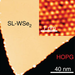
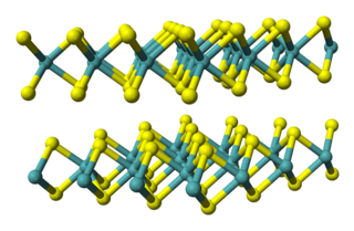
Tungsten diselenide is an inorganic compound with the formula WSe2. The compound adopts a hexagonal crystalline structure similar to molybdenum disulfide. The tungsten atoms are covalently bonded to six selenium ligands in a trigonal prismatic coordination sphere while each selenium is bonded to three tungsten atoms in a pyramidal geometry. The tungsten–selenium bond has a length of 0.2526 nm, and the distance between selenium atoms is 0.334 nm. It is a well studied example of a layered material. The layers stack together via van der Waals interactions. WSe2 is a very stable semiconductor in the group-VI transition metal dichalcogenides.

<span class="mw-page-title-main">Transition metal dichalcogenide monolayers</span> Thin semiconductors

Transition-metal dichalcogenide (TMD or TMDC) monolayers are atomically thin semiconductors of the type MX2, with M a transition-metal atom (Mo, W, etc.) and X a chalcogen atom (S, Se, or Te). One layer of M atoms is sandwiched between two layers of X atoms. They are part of the large family of so-called 2D materials, named so to emphasize their extraordinary thinness. For example, a MoS2 monolayer is only 6.5 Å thick. The key feature of these materials is the interaction of large atoms in the 2D structure as compared with first-row transition-metal dichalcogenides, e.g., WTe2 exhibits anomalous giant magnetoresistance and superconductivity.

A two-dimensional semiconductor is a type of natural semiconductor with thicknesses on the atomic scale. Geim and Novoselov et al. initiated the field in 2004 when they reported a new semiconducting material graphene, a flat monolayer of carbon atoms arranged in a 2D honeycomb lattice. A 2D monolayer semiconductor is significant because it exhibits stronger piezoelectric coupling than traditionally employed bulk forms. This coupling could enable applications. One research focus is on designing nanoelectronic components by the use of graphene as electrical conductor, hexagonal boron nitride as electrical insulator, and a transition metal dichalcogenide as semiconductor.

<span class="mw-page-title-main">Oxyselenide</span> Class of chemical compounds

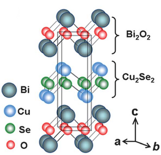
Oxyselenides are a group of chemical compounds that contain oxygen and selenium atoms. Oxyselenides can form a wide range of structures in compounds containing various transition metals, and thus can exhibit a wide range of properties. Most importantly, oxyselenides have a wide range of thermal conductivity, which can be controlled with changes in temperature in order to adjust their thermoelectric performance. Current research on oxyselenides indicates their potential for significant application in electronic materials.

<span class="mw-page-title-main">Molybdenum ditelluride</span> Chemical compound

Molybdenum(IV) telluride, molybdenum ditelluride or just molybdenum telluride is a compound of molybdenum and tellurium with formula MoTe2, corresponding to a mass percentage of 27.32% molybdenum and 72.68% tellurium.

<span class="mw-page-title-main">Niobium diselenide</span> Chemical compound

Niobium diselenide or niobium(IV) selenide is a layered transition metal dichalcogenide with formula NbSe2. Niobium diselenide is a lubricant, and a superconductor at temperatures below 7.2 K that exhibit a charge density wave (CDW). NbSe2 crystallizes in several related forms, and can be mechanically exfoliated into monatomic layers, similar to other transition metal dichalcogenide monolayers. Monolayer NbSe2 exhibits very different properties from the bulk material, such as of Ising superconductivity, quantum metallic state, and strong enhancement of the CDW.

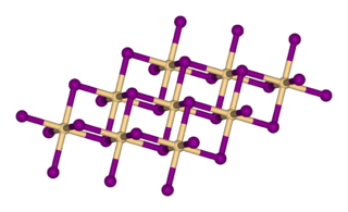
Verbeekite is a rare mineral consisting of palladium diselenide PdSe2. This transition metal dichalcogenide has an unusual monoclinic structure, with pairs of selenium atoms existing as dimers forming layers between palladium atom sheets. Unit cell dimensions are: a = 6.710, b = 4.154, c = 8.914 Å, β = 92.42 °, V = 248.24 Å3. Palladium diselenide has five polymorphs. Verbeekite can be synthesised at 11.5 GPa pressure and 1300 °C.

<span class="mw-page-title-main">Rhenium diselenide</span> Chemical compound

Rhenium diselenide is an inorganic compound with the formula ReSe2. It has a layered structure where atoms are strongly bonded within each layer. The layers are held together by weak Van der Waals bonds, and can be easily peeled off from the bulk material.

Indium(II) selenide (InSe) is an inorganic compound composed of indium and selenium. It is a III-VI layered semiconductor. The solid has a structure consisting of two-dimensional layers bonded together only by van der Waals forces. Each layer has the atoms in the order Se-In-In-Se.

The selenide iodides are chemical compounds that contain both selenide ions (Se2−) and iodide ions (I) and one or metal atoms. They are in the class of mixed anion compounds or chalcogenide halides.

<span class="mw-page-title-main">Tantalum diselenide</span> Chemical compound

Tantalum diselenide is a compound made with tantalum and selenium atoms, with chemical formula TaSe2, which belongs to the family of transition metal dichalcogenides. In contrast to molybdenum disulfide (MoS2) or rhenium disulfide (ReS2), tantalum diselenide does not occur spontaneously in nature, but it can be synthesized. Depending on the growth parameters, different types of crystal structures can be stabilized.

Germanium diselenide is an inorganic compound, with the chemical formula of GeSe2.

References

  1. Guo, G Y; Liang, W Y (10 March 1986). "The electronic structures of platinum dichalcogenides: PtS2 , PtSe2 and PtTe2". Journal of Physics C: Solid State Physics. 19 (7): 995–1008. Bibcode:1986JPhC...19..995G. doi:10.1088/0022-3719/19/7/011.
  2. 1 2 Grønvold, Fredrik; Haakon, Haraldsen; Kjekshus, Arne (1960). "On the sulfides, selenides and tellurides of platinum" (PDF). Acta Chemica Scandinavica . 14 (9): 1879–1893. doi: 10.3891/acta.chem.scand.14-1879 . Open Access logo PLoS transparent.svg
  3. 1 2 "Ultra-fast, ultra-sensitive PtSe2 gas sensors". PhysOrg. 13 January 2017. Retrieved 17 March 2017.
  4. Yim, Chanyoung; Lee, Kangho; McEvoy, Niall; O’Brien, Maria; Riazimehr, Sarah; Berner, Nina C.; Cullen, Conor P.; Kotakoski, Jani; Meyer, Jannik C.; Lemme, Max C.; Duesberg, Georg S. (25 October 2016). "High-Performance Hybrid Electronic Devices from Layered PtSe2 Films Grown at Low Temperature". ACS Nano. 10 (10): 9550–9558. arXiv: 1606.08673 . doi:10.1021/acsnano.6b04898. PMID   27661979. S2CID   22259155.
  5. 1 2 3 Wang, Yeliang; Li, Linfei; Yao, Wei; Song, Shiru; Sun, J. T.; Pan, Jinbo; Ren, Xiao; Li, Chen; Okunishi, Eiji; Wang, Yu-Qi; Wang, Eryin; Shao, Yan; Zhang, Y. Y.; Yang, Hai-tao; Schwier, Eike F.; Iwasawa, Hideaki; Shimada, Kenya; Taniguchi, Masaki; Cheng, Zhaohua; Zhou, Shuyun; Du, Shixuan; Pennycook, Stephen J.; Pantelides, Sokrates T.; Gao, Hong-Jun (10 June 2015). "Monolayer PtSe2, a New Semiconducting Transition-Metal-Dichalcogenide, Epitaxially Grown by Direct Selenization of Pt". Nano Letters. 15 (6): 4013–4018. Bibcode:2015NanoL..15.4013W. doi:10.1021/acs.nanolett.5b00964. OSTI   1185929. PMID   25996311.
  6. "Sudovikovite: Sudovikovite mineral information and data". www.mindat.org. Retrieved 19 March 2017.
  7. 1 2 3 4 O’Brien, Maria; McEvoy, Niall; Motta, Carlo; Zheng, Jian-Yao; Berner, Nina C; Kotakoski, Jani; Elibol, Kenan; Pennycook, Timothy J; Meyer, Jannik C; Yim, Chanyoung; Abid, Mohamed; Hallam, Toby; Donegan, John F; Sanvito, Stefano; Duesberg, Georg S (13 April 2016). "Raman characterization of platinum diselenide thin films". 2D Materials. 3 (2): 021004. arXiv: 1512.09317 . Bibcode:2016TDM.....3b1004O. doi:10.1088/2053-1583/3/2/021004. S2CID   119271642.
  8. Ciarrocchi, Alberto; Avsar, Ahmet; Ovchinnikov, Dmitry; Kis, Andras (2018-03-02). "Thickness-modulated metal-to-semiconductor transformation in a transition metal dichalcogenide". Nature Communications. 9 (1): 919. Bibcode:2018NatCo...9..919C. doi:10.1038/s41467-018-03436-0. ISSN   2041-1723. PMC   5834615 . PMID   29500434.
  9. 1 2 3 Zhao, Yuda; Qiao, Jingsi; Yu, Zhihao; Yu, Peng; Xu, Kang; Lau, Shu Ping; Zhou, Wu; Liu, Zheng; Wang, Xinran; Ji, Wei; Chai, Yang (February 2017). "High-Electron-Mobility and Air-Stable 2D Layered PtSe2 FETs". Advanced Materials. 29 (5): 1604230. doi:10.1002/adma.201604230. hdl:10397/65694. PMID   27886410. S2CID   9237296.
  10. Hulliger, F. (March 1965). "Electrical properties of some nickel-group chalcogenides". Journal of Physics and Chemistry of Solids. 26 (3): 639–645. Bibcode:1965JPCS...26..639H. doi:10.1016/0022-3697(65)90140-X.
  11. Zulfiqar, Muhammad; Zhao, Yinchang; Li, Geng; Nazir, Safdar; Ni, Jun (3 November 2016). "Tunable Conductivity and Half Metallic Ferromagnetism in Monolayer Platinum Diselenide: A First-Principles Study". The Journal of Physical Chemistry C. 120 (43): 25030–25036. doi:10.1021/acs.jpcc.6b06999.
  12. Avsar, Ahmet; Ciarrocchi, Alberto; Pizzochero, Michele; Unuchek, Dmitrii; Yazyev, Oleg V.; Kis, Andras (July 2019). "Defect induced, layer-modulated magnetism in ultrathin metallic PtSe2". Nature Nanotechnology. 14 (7): 674–678. Bibcode:2019NatNa..14..674A. doi:10.1038/s41565-019-0467-1. ISSN   1748-3387. PMC   6774792 . PMID   31209281.
  13. Yao, Wei; Wang, Eryin; Huang, Huaqing; Deng, Ke; Yan, Mingzhe; Zhang, Kenan; Miyamoto, Koji; Okuda, Taichi; Li, Linfei; Wang, Yeliang; Gao, Hongjun; Liu, Chaoxing; Duan, Wenhui; Zhou, Shuyun (31 January 2017). "Direct observation of spin-layer locking by local Rashba effect in monolayer semiconducting PtSe2 film". Nature Communications. 8: 14216. Bibcode:2017NatCo...814216Y. doi:10.1038/ncomms14216. PMC   5290424 . PMID   28139646.
  14. Dey, Sandip; Jain, Vimal K. (2004). "Platinum group metal chalcogenides" (PDF). Platinum Metals Review. 48 (1): 16–29. doi:10.1595/003214004X4811629. Open Access logo PLoS transparent.svg
  15. Oh, George N.; Choi, Eun Sang; Ibers, James A. (2 April 2012). "Syntheses and Characterization of Nine Quaternary Uranium Chalcogenides Among the Compounds A2 M3 UQ6(A = K, Rb, Cs; M = Pd, Pt; Q = S, Se)". Inorganic Chemistry. 51 (7): 4224–4230. doi:10.1021/ic2027048. PMID   22424143. S2CID   29859041.
  16. Drabek, M.; Vymazalova, A.; Cabral, A. R. (10 July 2012). "THE SYSTEM Hg-Pt-Se AT 400 C: PHASE RELATIONS INVOLVING JACUTINGAITE". The Canadian Mineralogist. 50 (2): 441–446. Bibcode:2012CaMin..50..441D. doi:10.3749/canmin.50.2.441.
  17. Zeng, Longhui; Han, Wei; Wu, Shuo-En; Wu, Di; Lau, Shu Ping; Tsang, Yuen Hong (November 2022). "Graphene/PtSe/Pyramid Si van Der Waals Schottky Junction for Room-Temperature Broadband Infrared Light Detection". IEEE Transactions on Electron Devices. 69 (11): 6212–6216. Bibcode:2022ITED...69.6212Z. doi:10.1109/TED.2022.3208854. S2CID   252739491.