


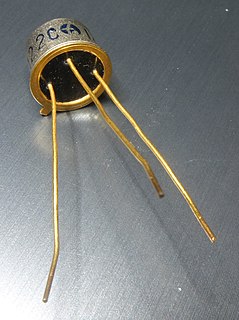
In electronics, TO-18 is a designation for a style of transistor metal case. The case is more expensive than the similarly sized plastic TO-92 package. The name is from JEDEC, signifying Transistor Outline Package, Case Style 18. [1]
In electronics, TO-18 is a designation for a style of transistor metal case. The case is more expensive than the similarly sized plastic TO-92 package. The name is from JEDEC, signifying Transistor Outline Package, Case Style 18. [1]
The typical TO-18 metal can package has a base diameter of 5.6 mm (0.22 in), a cap diameter of 4.70 mm (0.185 in), a cap height of 4.83 mm (0.190 in). [1] The tab is located 45° from pin 1, which is typically the emitter. The lead diameter is nominally 0.45 mm (0.018 in). The leads are arranged in a circle with a diameter of 2.54 mm (0.100 in). The minimum length of the leads is 12.7 mm (0.50 in).
Different manufacturers have different tolerances, and the actual form factor may vary slightly, depending on function.

The 3-lead TO-18 is used for transistors and other devices using no more than three leads. Variants for diodes, photodiodes and LEDs may have only two leads. Light-sensitive or light-emitting devices have a transparent window, lens, or parabolic reflectors in the top of the case rather than a sealed, flat top. For example, diode lasers such as those found in CD players may be packaged in TO-18 cases with a lens.
There are variants with between 2 and 8 leads.
The TO-46 [2] and TO-52 [3] packages have 3 leads. These packages differ from all other variants in the height of the cap. Instead of 4.83 mm (0.190 in) the cap height is only 3.30 mm (0.130 in) for TO-52 and 1.90 mm (0.075 in) for TO-46.
The package with 4 leads but otherwise with dimensions identical to TO-18, is standardized as TO-72. [4] The fourth wire is typically connected to the metal case as a means of electromagnetic shielding for radio frequency applications.
The TO-71 package has 8 leads (up to three of those may be omitted). [5] The minimum angle between two adjacent leads is 45°.
TO-206 is intended to replace previous definitions of packages with leads arranged in a circle with a diameter of 2.54 mm (0.100 in). [6] [7] The different outlines are now defined as variants of TO-206: TO-18 is renamed to TO-206-AA, TO-46 to TO-206-AB, TO-52 to TO-206-AC, TO-72 to TO-206-AF. A new package with 3 leads and a cap height of 1.40 mm (0.055 in) (i.e. smaller than TO-46) is added as TO-206-AD. TO-206-AE does not require a minimum diameter of the leads but is otherwise identical to TO-18. The somewhat unrelated TO-58 package is included as TO-206-AG.
| Standards organization | Standard | Designation for | |||
|---|---|---|---|---|---|
| TO-18 | TO-46 | TO-71 | TO-72 | ||
| JEDEC | JEP95 [7] | TO-206-AA | TO-206-AB | — | TO-206-AF |
| IEC | IEC 60191 [lower-alpha 1] [8] | C7/B11 | C10/B11 | C7/B12 | |
| DIN | DIN 41876 [9] [8] | 18A3 | 18A4 | ||
| EIAJ / JEITA | ED-7500A [lower-alpha 1] [10] | TC-7/TB-8C, TC-7/TB-16C | — | — | TC-7/TB-9C |
| British Standards | BS 3934 [lower-alpha 1] [11] [12] | SO-12A/SB3-6A | SO-12C/SB3-6A | SO-12A/SB8-1B | SO-12A/SB4-3 |
| Gosstandart | GOST 18472—88 [13] | KT-1-7 [lower-alpha 2] | KT-35-7 [lower-alpha 3] | — | KT-1-12 [lower-alpha 4] |
| Rosstandart | GOST R 57439 [14] | ||||
| Kombinat Mikroelektronik Erfurt | TGL 11811 [15] | A3/15-3a | — | — | A4/15-4a |
| TGL 26713/07 [15] | F1BA3 | — | — | F1CA3 | |

In microelectronics, a dual in-line package, is an electronic component package with a rectangular housing and two parallel rows of electrical connecting pins. The package may be through-hole mounted to a printed circuit board (PCB) or inserted in a socket. The dual-inline format was invented by Don Forbes, Rex Rice and Bryant Rogers at Fairchild R&D in 1964, when the restricted number of leads available on circular transistor-style packages became a limitation in the use of integrated circuits. Increasingly complex circuits required more signal and power supply leads ; eventually microprocessors and similar complex devices required more leads than could be put on a DIP package, leading to development of higher-density chip carriers. Furthermore, square and rectangular packages made it easier to route printed-circuit traces beneath the packages.
The JEDEC Solid State Technology Association is an independent semiconductor engineering trade organization and standardization body headquartered in Arlington County, Virginia, United States.
Pro Electron or EECA is the European type designation and registration system for active components.

Mullard Limited was a British manufacturer of electronic components. The Mullard Radio Valve Co. Ltd. of Southfields, London, was founded in 1920 by Captain Stanley R. Mullard, who had previously designed thermionic valves for the Admiralty before becoming managing director of the Z Electric Lamp Co. The company soon moved to Hammersmith, London and then in 1923 to Balham, London. The head office in later years was Mullard House at 1–19 Torrington Place, Bloomsbury, now part of University College London.

A small outline integrated circuit (SOIC) is a surface-mounted integrated circuit (IC) package which occupies an area about 30–50% less than an equivalent dual in-line package (DIP), with a typical thickness being 70% less. They are generally available in the same pin-outs as their counterpart DIP ICs. The convention for naming the package is SOIC or SO followed by the number of pins. For example, a 14-pin 4011 would be housed in an SOIC-14 or SO-14 package.
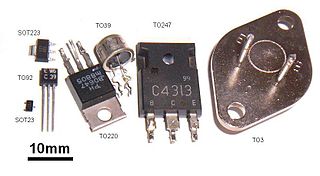
The TO-92 is a widely used style of semiconductor package mainly used for transistors. The case is often made of epoxy or plastic, and offers compact size at a very low cost.

The TO-220 is a style of electronic package used for high-powered, through-hole components with 0.1 inches (2.54 mm) pin spacing. The "TO" designation stands for "transistor outline". TO-220 packages have three leads. Similar packages with two, four, five or seven leads are also manufactured. A notable characteristic is a metal tab with a hole, used in mounting the case to a heatsink, allowing the component to dissipate more heat than one constructed in a TO-92 case. Common TO-220-packaged components include discrete semiconductors such as transistors and silicon-controlled rectifiers, as well as integrated circuits.

In electronics, TO-3 is a designation for a standardized metal semiconductor package used for power semiconductors, including transistors, silicon controlled rectifiers, and, integrated circuits. TO stands for "Transistor Outline" and relates to a series of technical drawings produced by JEDEC.

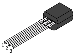
The 2N2222 is a common NPN bipolar junction transistor (BJT) used for general purpose low-power amplifying or switching applications. It is designed for low to medium current, low power, medium voltage, and can operate at moderately high speeds. It was originally made in the TO-18 metal can as shown in the picture.

The BC548 is a general-purpose NPN bipolar junction transistor commonly used in European and American electronic equipment. It is notably often the first type of bipolar transistor hobbyists encounter and is often featured in designs in hobby electronics magazines where a general-purpose transistor is required. The BC548 is low in cost and widely available.
A semiconductor package is a metal, plastic, glass, or ceramic casing containing one or more discrete semiconductor devices or integrated circuits. Individual components are fabricated on semiconductor wafers before being diced into die, tested, and packaged. The package provides a means for connecting it to the external environment, such as printed circuit board, via leads such as lands, balls, or pins; and protection against threats such as mechanical impact, chemical contamination, and light exposure. Additionally, it helps dissipate heat produced by the device, with or without the aid of a heat spreader. There are thousands of package types in use. Some are defined by international, national, or industry standards, while others are particular to an individual manufacturer.

DO-204 is a family of diode semiconductor packages defined by JEDEC. This family comprises lead-mounted axial devices with round leads. Generally a diode will have a line painted near the cathode end.

In electronics, a chip carrier is one of several kinds of surface-mount technology packages for integrated circuits. Connections are made on all four edges of a square package; compared to the internal cavity for mounting the integrated circuit, the package overall size is large.
A small outline transistor (SOT) is a family of small footprint, discrete surface mount transistor commonly used in consumer electronics. The most common SOT are SOT23 variations, also manufacturers offer the nearly identical thin small outline transistor (TSOT) package, where lower height is important.
In electronics, TO-5 is a designation for a standardized metal semiconductor package used for transistors and some integrated circuits. The TO element stands for "transistor outline" and refers to a series of technical drawings produced by JEDEC. The first commercial silicon transistors, the 2N696 and 2N697 from Fairchild Semiconductor, came in a TO-5 package.
Japanese Industrial Standards (JIS) has standard JIS-C-7012 for semiconductor part numbers. The first digit denotes the p-n junction count ; then follows the letter "S", then:

TO-126 is a type of semiconductor package for devices with three pins, such as transistors. The package is rectangular with a hole in the middle to allow for easy mounting to a board or a heat sink. On one side of the package typically a metal sheet is exposed, with the transistor die bonded to the other side of the metal sheet inside the package. This allows for an efficient heat transfer from the transistor die to an external heat sink but also implies that the metal sheet is electrically connected to the die.

TO-66 is a type of semiconductor package for devices with three connections, such as transistors. The shape is similar to the TO-3 package, but the size is smaller. The TO-66 package is made entirely of metal and is commonly used by silicon controlled rectifiers and power transistors. In Europe, it was popularly used by the complementary germanium power transistors AD161/AD162.
In electronics, TO-8 is a designation for a standardized metal semiconductor package. TO in TO-8 stands for "transistor outline" and refers to a series of technical drawings produced by JEDEC. The TO-8 package is noticeably larger than the more common TO-5 package. While originally designed for medium power transistors such as the 2N1483 series or the AD136, it is more commonly used for integrated circuits and sensors.
| Wikimedia Commons has media related to TO integrated circuit packages . |