
An integrated circuit or monolithic integrated circuit is a set of electronic circuits on one small flat piece of semiconductor material, usually silicon. Large numbers of tiny MOSFETs integrate into a small chip. This results in circuits that are orders of magnitude smaller, faster, and less expensive than those constructed of discrete electronic components. The IC's mass production capability, reliability, and building-block approach to integrated circuit design has ensured the rapid adoption of standardized ICs in place of designs using discrete transistors. ICs are now used in virtually all electronic equipment and have revolutionized the world of electronics. Computers, mobile phones and other home appliances are now inextricable parts of the structure of modern societies, made possible by the small size and low cost of ICs such as modern computer processors and microcontrollers.

Semiconductor device fabrication is the process used to manufacture semiconductor devices, typically integrated circuit (IC) chips such as modern computer processors, microcontrollers, and memory chips such as NAND flash and DRAM that are present in everyday electrical and electronic devices. It is a multiple-step sequence of photolithographic and chemical processing steps during which electronic circuits are gradually created on a wafer made of pure semiconducting material. Silicon is almost always used, but various compound semiconductors are used for specialized applications.

In microelectronics, a dual in-line package, is an electronic component package with a rectangular housing and two parallel rows of electrical connecting pins. The package may be through-hole mounted to a printed circuit board (PCB) or inserted in a socket. The dual-inline format was invented by Don Forbes, Rex Rice and Bryant Rogers at Fairchild R&D in 1964, when the restricted number of leads available on circular transistor-style packages became a limitation in the use of integrated circuits. Increasingly complex circuits required more signal and power supply leads ; eventually microprocessors and similar complex devices required more leads than could be put on a DIP package, leading to development of higher-density chip carriers. Furthermore, square and rectangular packages made it easier to route printed-circuit traces beneath the packages.

A ball grid array (BGA) is a type of surface-mount packaging used for integrated circuits. BGA packages are used to permanently mount devices such as microprocessors. A BGA can provide more interconnection pins than can be put on a dual in-line or flat package. The whole bottom surface of the device can be used, instead of just the perimeter. The traces connecting the package's leads to the wires or balls which connect the die to package are also on average shorter than with a perimeter-only type, leading to better performance at high speeds.

A pin grid array (PGA) is a type of integrated circuit packaging. In a PGA, the package is square or rectangular, and the pins are arranged in a regular array on the underside of the package. The pins are commonly spaced 2.54 mm (0.1") apart, and may or may not cover the entire underside of the package.

The 7400 series of integrated circuits (ICs) are a popular logic family of transistor–transistor logic (TTL) logic chips.

The 555 timer IC is an integrated circuit (chip) used in a variety of timer, delay, pulse generation, and oscillator applications. Derivatives provide two (556) or four (558) timing circuits in one package. The design was first marketed in 1972 by Signetics. Since then, numerous companies have made the original bipolar timers, as well as similar low-power CMOS timers. In 2017, it was said that over a billion 555 timers are produced annually by some estimates, and that the design was "probably the most popular integrated circuit ever made".
A quad flat package (QFP) is a surface-mounted integrated circuit package with "gull wing" leads extending from each of the four sides. Socketing such packages is rare and through-hole mounting is not possible. Versions ranging from 32 to 304 pins with a pitch ranging from 0.4 to 1.0 mm are common. Other special variants include low-profile QFP (LQFP) and thin QFP (TQFP).

A small outline integrated circuit (SOIC) is a surface-mounted integrated circuit (IC) package which occupies an area about 30–50% less than an equivalent dual in-line package (DIP), with a typical thickness being 70% less. They are generally available in the same pin-outs as their counterpart DIP ICs. The convention for naming the package is SOIC or SO followed by the number of pins. For example, a 14-pin 4011 would be housed in an SOIC-14 or SO-14 package.

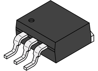
The TO-220 is a style of electronic package used for high-powered, through-hole components with 0.1 inches (2.54 mm) pin spacing. The "TO" designation stands for "transistor outline". TO-220 packages have three leads. Similar packages with two, four, five or seven leads are also manufactured. A notable characteristic is a metal tab with a hole, used in mounting the case to a heatsink, allowing the component to dissipate more heat than one constructed in a TO-92 case. Common TO-220-packaged components include discrete semiconductors such as transistors and silicon-controlled rectifiers, as well as integrated circuits.

In electronics, TO-3 is a designation for a standardized metal semiconductor package used for power semiconductors, including transistors, silicon controlled rectifiers, and, integrated circuits. TO stands for "Transistor Outline" and relates to a series of technical drawings produced by JEDEC.

In electronics, TO-18 is a designation for a style of transistor metal case. The case is more expensive than the similarly sized plastic TO-92 package. The name is from JEDEC, signifying Transistor Outline Package, Case Style 18.
The Double Decawatt Package, D2PAK, SOT404 or DDPAK, standardized as TO-263, refers to a semiconductor package type intended for surface mounting on circuit boards. The TO-263 is designed by Motorola. They are similar to the earlier TO-220-style packages intended for high power dissipation but lack the extended metal tab and mounting hole, while representing a larger version of the TO-252, also known as DPAK, SMT package. As with all SMT packages, the pins on a D2PAK are bent to lie against the PCB surface. The TO-263 can have 3 to 7 terminals.

In electronics, a chip carrier is one of several kinds of surface-mount technology packages for integrated circuits. Connections are made on all four edges of a square package; compared to the internal cavity for mounting the integrated circuit, the package overall size is large.
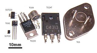
A small outline transistor (SOT) is a family of small footprint, discrete surface mount transistor commonly used in consumer electronics. The most common SOT are SOT23 variations, also manufacturers offer the nearly identical thin small outline transistor (TSOT) package, where lower height is important.
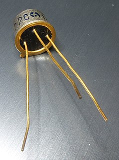
In electronics, TO-5 is a designation for a standardized metal semiconductor package used for transistors and some integrated circuits. The TO element stands for "transistor outline" and refers to a series of technical drawings produced by JEDEC. The first commercial silicon transistors, the 2N696 and 2N697 from Fairchild Semiconductor, came in a TO-5 package.

TO-126 is a type of semiconductor package for devices with three pins, such as transistors. The package is rectangular with a hole in the middle to allow for easy mounting to a board or a heat sink. On one side of the package typically a metal sheet is exposed, with the transistor die bonded to the other side of the metal sheet inside the package. This allows for an efficient heat transfer from the transistor die to an external heat sink but also implies that the metal sheet is electrically connected to the die.

TO-66 is a type of semiconductor package for devices with three connections, such as transistors. The shape is similar to the TO-3 package, but the size is smaller. The TO-66 package is made entirely of metal and is commonly used by silicon controlled rectifiers and power transistors. In Europe, it was popularly used by the complementary germanium power transistors AD161/AD162.
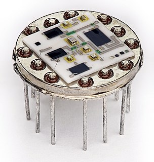
In electronics, TO-8 is a designation for a standardized metal semiconductor package. TO in TO-8 stands for "transistor outline" and refers to a series of technical drawings produced by JEDEC. The TO-8 package is noticeably larger than the more common TO-5 package. While originally designed for medium power transistors such as the 2N1483 series or the AD136, it is more commonly used for integrated circuits and sensors.

