Die singulation

Last updated

Die singulation, also called wafer dicing, is the process in semiconductor device fabrication by which dies are separated from a finished wafer of semiconductor. [1] Die singulation comes after the photolithography process. It can involve scribing and breaking, mechanical sawing (normally with a machine called a dicing saw ) [2] or laser cutting. All methods are typically automated to ensure precision and accuracy. [3] Following the dicing process the individual silicon chips may be encapsulated into chip carriers which are then suitable for use in building electronic devices such as computers, etc.

Contents

During dicing, wafers are typically mounted on dicing tape which has a sticky backing that holds the wafer on a thin sheet metal frame. Dicing tape has different properties depending on the dicing application. UV curable tapes are used for smaller sizes and non-UV dicing tape for larger die sizes. Dicing saws may use a dicing blade with diamond particles, rotating at 30,000 RPM and cooled with deionized water. Once a wafer has been diced, the pieces left on the dicing tape are referred to as die, dice or dies. Each will be packaged in a suitable package or placed directly on a printed circuit board substrate as a "bare die". The areas that have been cut away, called die streets, are typically about 75 micrometres (0.003 inch) wide. Once a wafer has been diced, the die will stay on the dicing tape until they are extracted by die-handling equipment, such as a die bonder or die sorter, further in the electronics assembly process.

Standard semiconductor manufacturing uses a "dicing after thinning" approach, where wafers are first thinned before they are diced. The wafer is ground down in a process called back side grinding (BSG) before it is diced. [1]

The size of the die left on the tape may range from 35 mm on a side (very large) to 0.1 mm square (very small). The die created may be any shape generated by straight lines, but they are typically rectangular or square-shaped. In some cases they can be other shapes as well depending on the singulation method used. A full-cut laser dicer has the ability to cut and separate in a variety of shapes.

Materials diced include glass, alumina, silicon, gallium arsenide (GaAs), silicon on sapphire (SoS), ceramics, and delicate compound semiconductors.[ citation needed ]

Stealth dicing

Cross sectional micrograph of cleavage plane after stealth dicing a Si wafer of 150 um thickness, compare Ref. Stealth diced Si wafer 150um 430x400 MB11.png
Cross sectional micrograph of cleavage plane after stealth dicing a Si wafer of 150 µm thickness, compare Ref.

Dicing of silicon wafers may also be performed by a laser-based technique, the so-called stealth dicing process. It works as a two-stage process in which defect regions are firstly introduced into the wafer by scanning the beam along intended cutting lines and secondly an underlying carrier membrane is expanded to induce fracture. [5]

The first step operates with a pulsed Nd:YAG laser, the wavelength of which (1064 nm) is well adapted to the electronic band gap of silicon (1.11  eV or 1117 nm), so that maximum absorption may well be adjusted by optical focusing. [6] Defect regions of about 10 µm width are inscribed by multiple scans of the laser along the intended dicing lanes, where the beam is focused at different depths of the wafer. [7] The figure displays an optical micrograph of a cleavage plane of a separated chip of 150 µm thickness that was subjected to four laser scans, compare. [4] The topmost defects are the best resolved and it is realized that a single laser pulse causes a defected crystal region that resembles the shape of candle flame. This shape is caused by the rapid melting and solidification of the irradiated region in the laser beam focus, where the temperature of only some µm3 small volumes suddenly rises to some 1000 K within nanoseconds and falls to ambient temperature again. [6] [7] The laser is typically pulsed by a frequency of about 100 kHz, while the wafer is moved with a velocity of about 1 m/s. A defected region of about 10 µm width is finally inscribed in the wafer, along which preferential fracture occurs under mechanical loading. The fracture is performed in the second step and operates by radially expanding the carrier membrane to which the wafer is attached. The cleavage initiates at the bottom and advances to the surface, so a high distortion density must be introduced at the bottom.[ clarification needed ][ citation needed ]

It is the advantage of the stealth dicing process that it does not require a cooling liquid. Dry dicing methods inevitably have to be applied for the preparation of certain microelectromechanical systems (MEMS), in particular, when these are intended for bioelectronic applications. [4] In addition, stealth dicing hardly generates debris and allows for improved exploitation of the wafer surface due to smaller kerf loss compared to wafer saw. Wafer grinding may be performed after this step, to reduce die thickness. [8]

Dice before grind

The DBG or "dice before grind" process is a way to separate dies without dicing. The separation occurs during the wafer thinning step. The wafers are initially diced using a half-cut dicer to a depth below the final target thickness. Next, the wafer is thinned to the target thickness while mounted on a special adhesive film [9] and then mounted on to a pick-up tape to hold the dies in place until they are ready for the packaging step. The benefit to the DBG process is higher die strength. [10] Alternatively, plasma dicing may be used, which replaces the dicer's saw with DRIE plasma etching. [11] [12] [13] [14] [15] [16] [17] [18]

The DBG process requires a back grinding tape that has the following attributes, 1) strong adhesive force (prevents infiltration of grinding fluid and die dust during grinding), 2) absorption and/or relief of compression stress and shear stress during grinding, 3) suppresses cracking due to contact between dies, 4) adhesive strength that can be greatly reduced through UV irradiation. [19]

See also

Related Research Articles

<span class="mw-page-title-main">Chemical vapor deposition</span> Method used to apply surface coatings

Chemical vapor deposition (CVD) is a vacuum deposition method used to produce high-quality, and high-performance, solid materials. The process is often used in the semiconductor industry to produce thin films.

<span class="mw-page-title-main">MEMS</span> Very small devices that incorporate moving components

MEMS is the technology of microscopic devices incorporating both electronic and moving parts. MEMS are made up of components between 1 and 100 micrometres in size, and MEMS devices generally range in size from 20 micrometres to a millimetre, although components arranged in arrays can be more than 1000 mm2. They usually consist of a central unit that processes data and several components that interact with the surroundings.

Photolithography is a process used in the manufacturing of integrated circuits. It involves using light to transfer a pattern onto a substrate, typically a silicon wafer.

<span class="mw-page-title-main">Semiconductor device fabrication</span> Manufacturing process used to create integrated circuits

Semiconductor device fabrication is the process used to manufacture semiconductor devices, typically integrated circuits (ICs) such as computer processors, microcontrollers, and memory chips that are present in everyday electronic devices. It is a multiple-step photolithographic and physio-chemical process during which electronic circuits are gradually created on a wafer, typically made of pure single-crystal semiconducting material. Silicon is almost always used, but various compound semiconductors are used for specialized applications.

<span class="mw-page-title-main">Wafer (electronics)</span> Thin slice of semiconductor used for the fabrication of integrated circuits

In electronics, a wafer is a thin slice of semiconductor, such as a crystalline silicon (c-Si), used for the fabrication of integrated circuits and, in photovoltaics, to manufacture solar cells.

<span class="mw-page-title-main">Laser cutting</span> Technology that uses a laser to cut materials

Laser cutting is a technology that uses a laser to vaporize materials, resulting in a cut edge. While typically used for industrial manufacturing applications, it is now used by schools, small businesses, architecture, and hobbyists. Laser cutting works by directing the output of a high-power laser most commonly through optics. The laser optics and CNC are used to direct the laser beam to the material. A commercial laser for cutting materials uses a motion control system to follow a CNC or G-code of the pattern to be cut onto the material. The focused laser beam is directed at the material, which then either melts, burns, vaporizes away, or is blown away by a jet of gas, leaving an edge with a high-quality surface finish.

<span class="mw-page-title-main">Die preparation</span>

Die preparation is a step of semiconductor device fabrication during which a wafer is prepared for IC packaging and IC testing. The process of die preparation typically consists of two steps: wafer mounting and wafer dicing.

An epitaxial wafer is a wafer of semiconducting material made by epitaxial growth (epitaxy) for use in photonics, microelectronics, spintronics, or photovoltaics. The epi layer may be the same material as the substrate, typically monocrystaline silicon, or it may be a silicon dioxide (SoI) or a more exotic material with specific desirable qualities. The purpose of epitaxy is to perfect the crystal structure over the bare substrate below and improve the wafer surface's electrical characteristics, making it suitable for highly complex microprocessors and memory devices.

Deep reactive-ion etching (DRIE) is a highly anisotropic etch process used to create deep penetration, steep-sided holes and trenches in wafers/substrates, typically with high aspect ratios. It was developed for microelectromechanical systems (MEMS), which require these features, but is also used to excavate trenches for high-density capacitors for DRAM and more recently for creating through silicon vias (TSVs) in advanced 3D wafer level packaging technology. In DRIE, the substrate is placed inside a reactor, and several gases are introduced. A plasma is struck in the gas mixture which breaks the gas molecules into ions. The ions accelerated towards, and react with the surface of the material being etched, forming another gaseous element. This is known as the chemical part of the reactive ion etching. There is also a physical part, if ions have enough energy, they can knock atoms out of the material to be etched without chemical reaction.

KLA Corporation is an American capital equipment company based in Milpitas, California. It supplies process control and yield management systems for the semiconductor industry and other related nanoelectronics industries. The company's products and services are intended for all phases of wafer, reticle, integrated circuit (IC) and packaging production, from research and development to final volume manufacturing.

<span class="mw-page-title-main">Microfabrication</span> Fabrication at micrometre scales and smaller

Microfabrication is the process of fabricating miniature structures of micrometre scales and smaller. Historically, the earliest microfabrication processes were used for integrated circuit fabrication, also known as "semiconductor manufacturing" or "semiconductor device fabrication". In the last two decades microelectromechanical systems (MEMS), microsystems, micromachines and their subfields, microfluidics/lab-on-a-chip, optical MEMS, RF MEMS, PowerMEMS, BioMEMS and their extension into nanoscale have re-used, adapted or extended microfabrication methods. Flat-panel displays and solar cells are also using similar techniques.

<span class="mw-page-title-main">Dicing saw</span> Type of saw

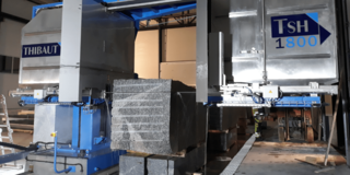
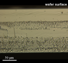
A dicing saw is a kind of saw which employs a high-speed spindle fitted with an extremely thin diamond blade or diamond wire to dice, cut, or groove semiconductor wafers, and glass, ceramic, crystal, and many other types of material.

<span class="mw-page-title-main">Disco Corporation</span>

DISCO Corporation is a Japanese precision tools maker, especially for the semiconductor production industry.

Adhesive bonding describes a wafer bonding technique with applying an intermediate layer to connect substrates of different types of materials. Those connections produced can be soluble or insoluble. The commercially available adhesive can be organic or inorganic and is deposited on one or both substrate surfaces. Adhesives, especially the well-established SU-8, and benzocyclobutene (BCB), are specialized for MEMS or electronic component production.

Monocrystalline silicon, more often called single-crystal silicon, in short mono c-Si or mono-Si, is the base material for silicon-based discrete components and integrated circuits used in virtually all modern electronic equipment. Mono-Si also serves as a photovoltaic, light-absorbing material in the manufacture of solar cells.

Wafer backgrinding is a semiconductor device fabrication step during which wafer thickness is reduced to allow stacking and high-density packaging of integrated circuits (IC).

<span class="mw-page-title-main">Crystalline silicon</span> Semiconducting material used in solar cell technology

Crystalline silicon or (c-Si) Is the crystalline forms of silicon, either polycrystalline silicon, or monocrystalline silicon. Crystalline silicon is the dominant semiconducting material used in photovoltaic technology for the production of solar cells. These cells are assembled into solar panels as part of a photovoltaic system to generate solar power from sunlight.

<span class="mw-page-title-main">Dicing tape</span> Special adhesive tape used during microchip manufacture

Dicing tape is a backing tape used during wafer dicing or some other microelectronic substrate separation, the cutting apart of pieces of semiconductor or other material following wafer or module microfabrication. The tape holds the pieces of the substrate, in case of a wafer called as die, together during the cutting process, mounting them to a thin metal frame. The dies/substrate pieces are removed from the dicing tape later on in the electronics manufacturing process.

Ultra-high-purity steam, also called the clean steam, UHP steam or high purity water vapor, is used in a variety of industrial manufacturing processes that require oxidation or annealing. These processes include the growth of oxide layers on silicon wafers for the semiconductor industry, originally described by the Deal-Grove model, and for the formation of passivation layers used to improve the light capture ability of crystalline photovoltaic cells. Several methods and technologies can be employed to generate ultra high purity steam, including pyrolysis, bubbling, direct liquid injection, and purified steam generation. The level of purity, or the relative lack of contamination, affects the quality of the oxide layer or annealed surface. The method of delivery affects growth rate, uniformity, and electrical performance. Oxidation and annealing are common steps in the manufacture of such devices as microelectronics and solar cells.

Glossary of microelectronics manufacturing terms

References

  1. 1 2 Lei, Wei-Sheng; Kumar, Ajay; Yalamanchili, Rao (2012-04-06). "Die singulation technologies for advanced packaging: A critical review". Journal of Vacuum Science & Technology B, Nanotechnology and Microelectronics: Materials, Processing, Measurement, and Phenomena. 30 (4): 040801. Bibcode:2012JVSTB..30d0801L. doi:10.1116/1.3700230. ISSN   2166-2746.
  2. "Key Wafer Sawing Factors". Optocap. Archived from the original on 21 May 2013. Retrieved 14 April 2013.
  3. "Wafer Dicing Service | Wafer Backgrinding & Bonding Services". www.syagrussystems.com. Retrieved 2021-11-20.
  4. 1 2 3 M. Birkholz; K.-E. Ehwald; M. Kaynak; T. Semperowitsch; B. Holz; S. Nordhoff (2010). "Separation of extremely miniaturized medical sensors by IR laser dicing". J. Opto. Adv. Mat. 12: 479–483.
  5. M. Kumagai; N. Uchiyama; E. Ohmura; R. Sugiura; K. Atsumi; K. Fukumitsu (August 2007). "Advanced Dicing Technology for Semiconductor Wafer—Stealth Dicing". IEEE Transactions on Semiconductor Manufacturing. 20 (3): 259–265. doi:10.1109/TSM.2007.901849. S2CID   6034954.
  6. 1 2 E. Ohmura; F. Fukuyo; K. Fukumitsu; H. Morita (2006). "Internal modified layer formation mechanism into silicon with nanosecond laser". J. Achiev. Mat. Manuf. Eng. 17: 381–384.
  7. 1 2 M. Kumagai; N. Uchiyama; E. Ohmura; R. Sugiura; K. Atsumi; K. Fukumitsu (2007). "Advanced Dicing Technology for Semiconductor Wafer – Stealth Dicing". IEEE Transactions on Semiconductor Manufacturing. 20 (3): 259–265. doi:10.1109/TSM.2007.901849. S2CID   6034954.
  8. "共通 | DISCO Corporation".
  9. "共通 | DISCO Corporation".
  10. "Semiconductor Dicing Tapes". Semiconductor Dicing Tapes. Retrieved 14 April 2013.
  11. "Plasma Dicing | Orbotech". www.orbotech.com.
  12. "APX300 : Plasma Dicer - Industrial Devices & Solutions - Panasonic". industrial.panasonic.com.
  13. "Plasma Dicing of Silicon & III-V (GaAs, InP & GaN)". SAMCO Inc.
  14. "Example of plasma dicing process | Download Scientific Diagram".
  15. "Plasma-Therm: Plasma Dicing". www.plasmatherm.com. Archived from the original on 2023-03-06. Retrieved 2019-05-26.
  16. "Plasma Dicing Solutions of a Variety of Materials: From Silicon Wafers with Metal or Resin Layers, to Compound Semiconductors" (PDF). Retrieved 2023-11-19.
  17. "Resource Center". Plasma-Therm. June 22, 2022.
  18. "Plasma Dicing (Dice Before Grind) | Orbotech". www.orbotech.com.
  19. Products for DBG Process (LINTEC) http://www.lintec-usa.com/di_dbg.cfm