An electron microscope is a microscope that uses a beam of electrons as a source of illumination. They use electron optics that are analogous to the glass lenses of an optical light microscope to control the electron beam, for instance focusing them to produce magnified images or electron diffraction patterns. As the wavelength of an electron can be up to 100,000 times smaller than that of visible light, electron microscopes have a much higher resolution of about 0.1 nm, which compares to about 200 nm for light microscopes. Electron microscope may refer to:

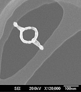
A scanning electron microscope (SEM) is a type of electron microscope that produces images of a sample by scanning the surface with a focused beam of electrons. The electrons interact with atoms in the sample, producing various signals that contain information about the surface topography and composition of the sample. The electron beam is scanned in a raster scan pattern, and the position of the beam is combined with the intensity of the detected signal to produce an image. In the most common SEM mode, secondary electrons emitted by atoms excited by the electron beam are detected using a secondary electron detector. The number of secondary electrons that can be detected, and thus the signal intensity, depends, among other things, on specimen topography. Some SEMs can achieve resolutions better than 1 nanometer.

Cathodoluminescence is an optical and electromagnetic phenomenon in which electrons impacting on a luminescent material such as a phosphor, cause the emission of photons which may have wavelengths in the visible spectrum. A familiar example is the generation of light by an electron beam scanning the phosphor-coated inner surface of the screen of a television that uses a cathode ray tube. Cathodoluminescence is the inverse of the photoelectric effect, in which electron emission is induced by irradiation with photons.

Transmission electron microscopy (TEM) is a microscopy technique in which a beam of electrons is transmitted through a specimen to form an image. The specimen is most often an ultrathin section less than 100 nm thick or a suspension on a grid. An image is formed from the interaction of the electrons with the sample as the beam is transmitted through the specimen. The image is then magnified and focused onto an imaging device, such as a fluorescent screen, a layer of photographic film, or a sensor such as a scintillator attached to a charge-coupled device.

A cathodoluminescence (CL) microscope combines methods from electron and regular microscopes. It is designed to study the luminescence characteristics of polished thin sections of solids irradiated by an electron beam.
A thin film is a layer of material ranging from fractions of a nanometer (monolayer) to several micrometers in thickness. The controlled synthesis of materials as thin films is a fundamental step in many applications. A familiar example is the household mirror, which typically has a thin metal coating on the back of a sheet of glass to form a reflective interface. The process of silvering was once commonly used to produce mirrors, while more recently the metal layer is deposited using techniques such as sputtering. Advances in thin film deposition techniques during the 20th century have enabled a wide range of technological breakthroughs in areas such as magnetic recording media, electronic semiconductor devices, integrated passive devices, LEDs, optical coatings, hard coatings on cutting tools, and for both energy generation and storage. It is also being applied to pharmaceuticals, via thin-film drug delivery. A stack of thin films is called a multilayer.

Self-assembled monolayers (SAM) of organic molecules are molecular assemblies formed spontaneously on surfaces by adsorption and are organized into more or less large ordered domains. In some cases molecules that form the monolayer do not interact strongly with the substrate. This is the case for instance of the two-dimensional supramolecular networks of e.g. perylenetetracarboxylic dianhydride (PTCDA) on gold or of e.g. porphyrins on highly oriented pyrolitic graphite (HOPG). In other cases the molecules possess a head group that has a strong affinity to the substrate and anchors the molecule to it. Such a SAM consisting of a head group, tail and functional end group is depicted in Figure 1. Common head groups include thiols, silanes, phosphonates, etc.

Alec Nigel Broers, Baron Broers, is a British electrical engineer.

A scanning transmission electron microscope (STEM) is a type of transmission electron microscope (TEM). Pronunciation is [stɛm] or [ɛsti:i:ɛm]. As with a conventional transmission electron microscope (CTEM), images are formed by electrons passing through a sufficiently thin specimen. However, unlike CTEM, in STEM the electron beam is focused to a fine spot which is then scanned over the sample in a raster illumination system constructed so that the sample is illuminated at each point with the beam parallel to the optical axis. The rastering of the beam across the sample makes STEM suitable for analytical techniques such as Z-contrast annular dark-field imaging, and spectroscopic mapping by energy dispersive X-ray (EDX) spectroscopy, or electron energy loss spectroscopy (EELS). These signals can be obtained simultaneously, allowing direct correlation of images and spectroscopic data.
Nanolithography (NL) is a growing field of techniques within nanotechnology dealing with the engineering of nanometer-scale structures on various materials.

Dip pen nanolithography (DPN) is a scanning probe lithography technique where an atomic force microscope (AFM) tip is used to create patterns directly on a range of substances with a variety of inks. A common example of this technique is exemplified by the use of alkane thiolates to imprint onto a gold surface. This technique allows surface patterning on scales of under 100 nanometers. DPN is the nanotechnology analog of the dip pen, where the tip of an atomic force microscope cantilever acts as a "pen", which is coated with a chemical compound or mixture acting as an "ink", and put in contact with a substrate, the "paper".

Focused ion beam, also known as FIB, is a technique used particularly in the semiconductor industry, materials science and increasingly in the biological field for site-specific analysis, deposition, and ablation of materials. A FIB setup is a scientific instrument that resembles a scanning electron microscope (SEM). However, while the SEM uses a focused beam of electrons to image the sample in the chamber, a FIB setup uses a focused beam of ions instead. FIB can also be incorporated in a system with both electron and ion beam columns, allowing the same feature to be investigated using either of the beams. FIB should not be confused with using a beam of focused ions for direct write lithography. These are generally quite different systems where the material is modified by other mechanisms.

A scanning helium ion microscope is an imaging technology based on a scanning helium ion beam. Similar to other focused ion beam techniques, it allows to combine milling and cutting of samples with their observation at sub-nanometer resolution.

Sputter deposition is a physical vapor deposition (PVD) method of thin film deposition by the phenomenon of sputtering. This involves ejecting material from a "target" that is a source onto a "substrate" such as a silicon wafer. Resputtering is re-emission of the deposited material during the deposition process by ion or atom bombardment. Sputtered atoms ejected from the target have a wide energy distribution, typically up to tens of eV. The sputtered ions can ballistically fly from the target in straight lines and impact energetically on the substrates or vacuum chamber. Alternatively, at higher gas pressures, the ions collide with the gas atoms that act as a moderator and move diffusively, reaching the substrates or vacuum chamber wall and condensing after undergoing a random walk. The entire range from high-energy ballistic impact to low-energy thermalized motion is accessible by changing the background gas pressure. The sputtering gas is often an inert gas such as argon. For efficient momentum transfer, the atomic weight of the sputtering gas should be close to the atomic weight of the target, so for sputtering light elements neon is preferable, while for heavy elements krypton or xenon are used. Reactive gases can also be used to sputter compounds. The compound can be formed on the target surface, in-flight or on the substrate depending on the process parameters. The availability of many parameters that control sputter deposition make it a complex process, but also allow experts a large degree of control over the growth and microstructure of the film.

Nanometrology is a subfield of metrology, concerned with the science of measurement at the nanoscale level. Nanometrology has a crucial role in order to produce nanomaterials and devices with a high degree of accuracy and reliability in nanomanufacturing.
Lisa McElwee-White is currently the Colonel Allen R. and Margaret G. Crow Professor of Chemistry at the University of Florida.

Liquid-phase electron microscopy refers to a class of methods for imaging specimens in liquid with nanometer spatial resolution using electron microscopy. LP-EM overcomes the key limitation of electron microscopy: since the electron optics requires a high vacuum, the sample must be stable in a vacuum environment. Many types of specimens relevant to biology, materials science, chemistry, geology, and physics, however, change their properties when placed in a vacuum.
A probe tip is an instrument used in scanning probe microscopes (SPMs) to scan the surface of a sample and make nano-scale images of surfaces and structures. The probe tip is mounted on the end of a cantilever and can be as sharp as a single atom. In microscopy, probe tip geometry and the composition of both the tip and the surface being probed directly affect resolution and imaging quality. Tip size and shape are extremely important in monitoring and detecting interactions between surfaces. SPMs can precisely measure electrostatic forces, magnetic forces, chemical bonding, Van der Waals forces, and capillary forces. SPMs can also reveal the morphology and topography of a surface.

Multi-tip scanning tunneling microscopy extends scanning tunneling microscopy (STM) from imaging to dedicated electrical measurements at the nanoscale like a ″multimeter at the nanoscale″. In materials science, nanoscience, and nanotechnology, it is desirable to measure electrical properties at a particular position of the sample. For this purpose, multi-tip STMs in which several tips are operated independently have been developed. Apart from imaging the sample, the tips of a multi-tip STM are used to form contacts to the sample at desired locations and to perform local electrical measurements.
Transmission Kikuchi Diffraction (TKD), also sometimes called transmission-electron backscatter diffraction (t-EBSD), is a method for orientation mapping at the nanoscale. It’s used for analysing the microstructures of thin transmission electron microscopy (TEM) specimens in the scanning electron microscope (SEM). This technique has been widely utilised in the characterization of nano-crystalline materials, including oxides, superconductors, and metallic alloys.