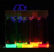
Quantum dots (QDs) or semiconductor nanocrystals are semiconductor particles a few nanometres in size with optical and electronic properties that differ from those of larger particles via quantum mechanical effects. They are a central topic in nanotechnology and materials science. When a quantum dot is illuminated by UV light, an electron in the quantum dot can be excited to a state of higher energy. In the case of a semiconducting quantum dot, this process corresponds to the transition of an electron from the valence band to the conductance band. The excited electron can drop back into the valence band releasing its energy as light. This light emission (photoluminescence) is illustrated in the figure on the right. The color of that light depends on the energy difference between the conductance band and the valence band, or the transition between discrete energy states when the band structure is no longer well-defined in QDs.
A selenide is a chemical compound containing a selenium with oxidation number of −2. Similar to sulfide, selenides occur both as inorganic compounds and as organic derivatives, which are called organoselenium compound.

Cadmium selenide is an inorganic compound with the formula CdSe. It is a black to red-black solid that is classified as a II-VI semiconductor of the n-type. It is a pigment but applications are declining because of environmental concerns

Copper indium gallium (di)selenide (CIGS) is a I-III-VI2 semiconductor material composed of copper, indium, gallium, and selenium. The material is a solid solution of copper indium selenide (often abbreviated "CIS") and copper gallium selenide. It has a chemical formula of CuIn1−xGaxSe2, where the value of x can vary from 0 (pure copper indium selenide) to 1 (pure copper gallium selenide). CIGS is a tetrahedrally bonded semiconductor, with the chalcopyrite crystal structure, and a bandgap varying continuously with x from about 1.0 eV (for copper indium selenide) to about 1.7 eV (for copper gallium selenide).

Phosphorene is a two-dimensional material consisting of phosphorus. It consists of a single layer of black phosphorus, the most stable allotrope of phosphorus. Phosphorene is analogous to graphene. Among two-dimensional materials, phosphorene is a competitor to graphene because it has a nonzero fundamental band gap that can be modulated by strain and the number of layers in a stack. Phosphorene was first isolated in 2014 by mechanical exfoliation. Liquid exfoliation is a promising method for scalable phosphorene production.
Lead selenide (PbSe), or lead(II) selenide, a selenide of lead, is a semiconductor material. It forms cubic crystals of the NaCl structure; it has a direct bandgap of 0.27 eV at room temperature. A grey solid, it is used for manufacture of infrared detectors for thermal imaging. The mineral clausthalite is a naturally occurring lead selenide.

Tin selenide, also known as stannous selenide, is an inorganic compound with the formula SnSe. Tin(II) selenide is a typical layered metal chalcogenide as it includes a group 16 anion (Se2−) and an electropositive element (Sn2+), and is arranged in a layered structure. Tin(II) selenide is a narrow band-gap (IV-VI) semiconductor structurally analogous to black phosphorus. It has received considerable interest for applications including low-cost photovoltaics, and memory-switching devices.
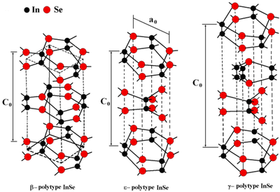
The indium chalcogenides include all compounds of indium with the chalcogen elements, oxygen, sulfur, selenium and tellurium. (Polonium is excluded as little is known about its compounds with indium). The best-characterised compounds are the In(III) and In(II) chalcogenides e.g. the sulfides In2S3 and InS.
This group of compounds has attracted a lot of research attention because they include semiconductors, photovoltaics and phase-change materials. In many applications indium chalcogenides are used as the basis of ternary and quaternary compounds such as indium tin oxide, ITO and copper indium gallium selenide, CIGS.
Tin(II) sulfide is a chemical compound of tin and sulfur. The chemical formula is SnS. Its natural occurrence concerns herzenbergite (α-SnS), a rare mineral. At elevated temperatures above 905 K, SnS undergoes a second order phase transition to β-SnS (space group: Cmcm, No. 63). In recent years, it has become evident that a new polymorph of SnS exists based upon the cubic crystal system, known as π-SnS (space group: P213, No. 198).
Gallium(II) selenide (GaSe) is a chemical compound. It has a hexagonal layer structure, similar to that of GaS. It is a photoconductor, a second harmonic generation crystal in nonlinear optics, and has been used as a far-infrared conversion material at 14–31 THz and above.
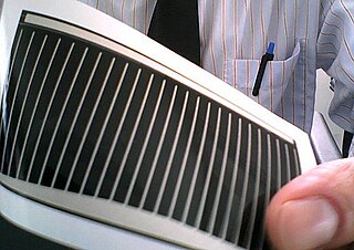
A copper indium gallium selenide solar cell is a thin-film solar cell used to convert sunlight into electric power. It is manufactured by depositing a thin layer of copper indium gallium selenide solid solution on glass or plastic backing, along with electrodes on the front and back to collect current. Because the material has a high absorption coefficient and strongly absorbs sunlight, a much thinner film is required than of other semiconductor materials.
Bismuth selenide is a gray compound of bismuth and selenium also known as bismuth(III) selenide.

Solar Frontier Kabushiki Kaisha is a Japanese photovoltaic company that develops and manufactures thin film solar cells using CIGS technology. It is a fully owned subsidiary of Showa Shell Sekiyu and located in Minato, Tokyo, Japan. The company was founded in 2006 as Showa Shell Solar, and renamed Solar Frontier in April 2010.
Iron(II) selenide refers to a number of inorganic compounds of ferrous iron and selenide (Se2−). The phase diagram of the system Fe–Se reveals the existence of several non-stoichiometric phases between ~49 at. % Se and ~53 at. % Fe, and temperatures up to ~450 °C. The low temperature stable phases are the tetragonal PbO-structure (P4/nmm) β-Fe1−xSe and α-Fe7Se8. The high temperature phase is the hexagonal, NiAs structure (P63/mmc) δ-Fe1−xSe. Iron(II) selenide occurs naturally as the NiAs-structure mineral achavalite.
Molybdenum diselenide is an inorganic compound of molybdenum and selenium. Its structure is similar to that of MoS
2. Compounds of this category are known as transition metal dichalcogenides, abbreviated TMDCs. These compounds, as the name suggests, are made up of a transition metals and elements of group 16 on the periodic table of the elements. Compared to MoS
2, MoSe
2 exhibits higher electrical conductivity.
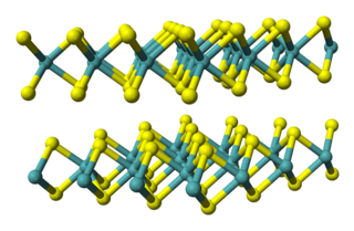
Tungsten diselenide is an inorganic compound with the formula WSe2. The compound adopts a hexagonal crystalline structure similar to molybdenum disulfide. The tungsten atoms are covalently bonded to six selenium ligands in a trigonal prismatic coordination sphere while each selenium is bonded to three tungsten atoms in a pyramidal geometry. The tungsten–selenium bond has a length of 0.2526 nm, and the distance between selenium atoms is 0.334 nm. It is a well studied example of a layered material. The layers stack together via van der Waals interactions. WSe2 is a very stable semiconductor in the group-VI transition metal dichalcogenides.
A two-dimensional semiconductor is a type of natural semiconductor with thicknesses on the atomic scale. Geim and Novoselov et al. initiated the field in 2004 when they reported a new semiconducting material graphene, a flat monolayer of carbon atoms arranged in a 2D honeycomb lattice. A 2D monolayer semiconductor is significant because it exhibits stronger piezoelectric coupling than traditionally employed bulk forms. This coupling could enable applications. One research focus is on designing nanoelectronic components by the use of graphene as electrical conductor, hexagonal boron nitride as electrical insulator, and a transition metal dichalcogenide as semiconductor.
Copper selenide is an inorganic binary compound between copper and selenium. The chemical formula depends on the ratio between the two elements, such as CuSe or Cu2Se.
Platinum diselenide is a transition metal dichalcogenide with the formula PtSe2. It is a layered substance that can be split into layers down to three atoms thick. PtSe2 can behave as a metalloid or as a semiconductor depending on the thickness.

Niobium diselenide or niobium(IV) selenide is a layered transition metal dichalcogenide with formula NbSe2. Niobium diselenide is a lubricant, and a superconductor at temperatures below 7.2 K that exhibit a charge density wave (CDW). NbSe2 crystallizes in several related forms, and can be mechanically exfoliated into monatomic layers, similar to other transition metal dichalcogenide monolayers. Monolayer NbSe2 exhibits very different properties from the bulk material, such as of Ising superconductivity, quantum metallic state, and strong enhancement of the CDW.