
Xeon is a brand of x86 microprocessors designed, manufactured, and marketed by Intel, targeted at the non-consumer workstation, server, and embedded markets. It was introduced in June 1998. Xeon processors are based on the same architecture as regular desktop-grade CPUs, but have advanced features such as support for error correction code (ECC) memory, higher core counts, more PCI Express lanes, support for larger amounts of RAM, larger cache memory and extra provision for enterprise-grade reliability, availability and serviceability (RAS) features responsible for handling hardware exceptions through the Machine Check Architecture (MCA). They are often capable of safely continuing execution where a normal processor cannot due to these extra RAS features, depending on the type and severity of the machine-check exception (MCE). Some also support multi-socket systems with two, four, or eight sockets through use of the Ultra Path Interconnect (UPI) bus.

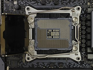
The land grid array (LGA) is a type of surface-mount packaging for integrated circuits (ICs) that is notable for having the pins on the socket — as opposed to pins on the integrated circuit, known as a pin grid array (PGA). An LGA can be electrically connected to a printed circuit board (PCB) either by the use of a socket or by soldering directly to the board.
The Intel QuickPath Interconnect (QPI) is a point-to-point processor interconnect developed by Intel which replaced the front-side bus (FSB) in Xeon, Itanium, and certain desktop platforms starting in 2008. It increased the scalability and available bandwidth. Prior to the name's announcement, Intel referred to it as Common System Interface (CSI). Earlier incarnations were known as Yet Another Protocol (YAP) and YAP+.

LGA 1366, also known as Socket B, is an Intel CPU socket. This socket supersedes Intel's LGA 775 in the high-end and performance desktop segments. It also replaces the server-oriented LGA 771 in the entry level and is superseded itself by LGA 2011. This socket has 1,366 protruding pins which touch contact points on the underside of the processor (CPU) and accesses up to three channels of DDR3 memory via the processor's internal memory controller.

LGA 2011, also called Socket R, is a CPU socket by Intel released on November 14, 2011. It launched along with LGA 1356 to replace its predecessor, LGA 1366 and LGA 1567. While LGA 1356 was designed for dual-processor or low-end servers, LGA 2011 was designed for high-end desktops and high-performance servers. The socket has 2011 protruding pins that touch contact points on the underside of the processor.

LGA 1356, also called Socket B2, is an Intel microprocessor socket released in Q1 2012 with 1356 Land Grid Array pins. It launched alongside LGA 2011 to replace its predecessor, LGA 1366 and LGA 1567. It's compatible with Intel Sandy Bridge-EN and Ivy Bridge-EN microprocessors.

Skylake is Intel's codename for its sixth generation Core microprocessor family that was launched on August 5, 2015, succeeding the Broadwell microarchitecture. Skylake is a microarchitecture redesign using the same 14 nm manufacturing process technology as its predecessor, serving as a tock in Intel's tick–tock manufacturing and design model. According to Intel, the redesign brings greater CPU and GPU performance and reduced power consumption. Skylake CPUs share their microarchitecture with Kaby Lake, Coffee Lake, Cannon Lake, Whiskey Lake, and Comet Lake CPUs.

Xeon Phi was a series of x86 manycore processors designed and made by Intel. It was intended for use in supercomputers, servers, and high-end workstations. Its architecture allowed use of standard programming languages and application programming interfaces (APIs) such as OpenMP.

Broadwell is the fifth generation of the Intel Core processor. It is Intel's codename for the 14 nanometer die shrink of its Haswell microarchitecture. It is a "tick" in Intel's tick–tock principle as the next step in semiconductor fabrication. Like some of the previous tick-tock iterations, Broadwell did not completely replace the full range of CPUs from the previous microarchitecture (Haswell), as there were no low-end desktop CPUs based on Broadwell.
AVX-512 are 512-bit extensions to the 256-bit Advanced Vector Extensions SIMD instructions for x86 instruction set architecture (ISA) proposed by Intel in July 2013, and first implemented in the 2016 Intel Xeon Phi x200, and then later in a number of AMD and other Intel CPUs. AVX-512 consists of multiple extensions that may be implemented independently. This policy is a departure from the historical requirement of implementing the entire instruction block. Only the core extension AVX-512F is required by all AVX-512 implementations.

LGA 1151, also known as Socket H4, is a type of zero insertion force flip-chip land grid array (LGA) socket for Intel desktop processors which comes in two distinct versions: the first revision which supports both Intel's Skylake and Kaby Lake CPUs, and the second revision which supports Coffee Lake CPUs exclusively.
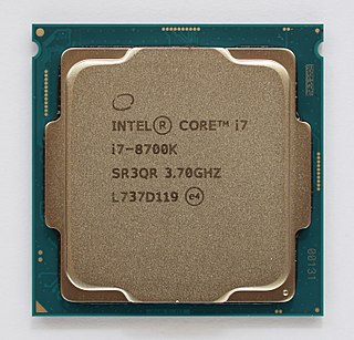
Coffee Lake is Intel's codename for its eighth-generation Core microprocessor family, announced on September 25, 2017. It is manufactured using Intel's second 14 nm process node refinement. Desktop Coffee Lake processors introduced i5 and i7 CPUs featuring six cores and Core i3 CPUs with four cores and no hyperthreading.
LGA 2066, also called Socket R4, is a CPU socket by Intel that debuted with Skylake-X and Kaby Lake-X processors in June 2017. It replaces Intel's LGA 2011-3 (R3) in the performance, high-end desktop and Workstation platforms, while LGA 3647 replaces LGA 2011-3 (R3) in the server platforms based on Skylake-SP.
The Intel Ultra Path Interconnect (UPI) is a point-to-point processor interconnect developed by Intel which replaced the Intel QuickPath Interconnect (QPI) in Xeon Skylake-SP platforms starting in 2017.
Sapphire Rapids is a codename for Intel's server and workstation processors based on the Golden Cove microarchitecture and produced using Intel 7. It features up to 60 cores and an array of accelerators.

Cascade Lake is an Intel codename for a 14 nm server, workstation and enthusiast processor generation, launched in April 2019. In Intel's process–architecture–optimization model, Cascade Lake is an optimization of Skylake. Intel states that this will be their first generation to support 3D XPoint-based memory modules. It also features Deep Learning Boost (DPL) instructions and mitigations for Meltdown and Spectre. Intel officially launched new Xeon Scalable SKUs on February 24, 2020.
Comet Lake is Intel's codename for its 10th generation Core processors. They are manufactured using Intel's third 14 nm Skylake process revision, succeeding the Whiskey Lake U-series mobile processor and Coffee Lake desktop processor families. Intel announced low-power mobile Comet Lake-U CPUs on August 21, 2019, H-series mobile CPUs on April 2, 2020, desktop Comet Lake-S CPUs April 30, 2020, and Xeon W-1200 series workstation CPUs on May 13, 2020. Comet Lake processors and Ice Lake 10 nm processors are together branded as the Intel "10th Generation Core" family. Intel officially launched Comet Lake-Refresh CPUs on the same day as 11th Gen Core Rocket Lake launch. The low-power mobile Comet Lake-U Core and Celeron 5205U CPUs were discontinued on July 7, 2021.
Cooper Lake is Intel's codename for the third-generation of their Xeon Scalable processors, developed as the successor to Cascade Lake-SP. Cooper Lake processors are targeted at the 4S and 8S segments of the server market; Ice Lake-SP serves the 1S and 2S segment.

LGA 1700 is a zero insertion force flip-chip land grid array (LGA) socket, compatible with Intel desktop processors Alder Lake and Raptor Lake, which was first released in November 2021.
