Xeon Phi

Last updated

Xeon Phi
Intel Xeon Phi 5100.jpg
Xeon Phi 5100 without heatsink
General information
Launched2010
Discontinued2020 [1]
Marketed byIntel
Designed byIntel
Common manufacturer(s)
  • Intel
Performance
Max. CPU clock rate 1.053 GHz to 1.7 GHz
Cache
L1 cache 32  KB per core
L2 cache512  KB per core
Architecture and classification
ApplicationSupercomputers
High-performance computing
Technology node 45 nm transistors to 14 nm transistors (tri-gate)
Microarchitecture Larrabee
Instruction set x86-16 (except coprocessor form factor), IA-32, x86-64 [2]
Extensions
Physical specifications
Cores
  • 32-72
Memory (RAM)
  • Up to 384 GB and 16 GB
  • Up to DDR4 115.4 GB/s with ECC support
  • MCDRAM 400+ GB/s
Socket(s)
Products, models, variants
Core name(s)
  • Knights Ferry
  • Knights Corner
  • Knights Landing
  • Knights Mill
  • Knights Hill
Model(s)
    • Xeon Phi 3100
    • Xeon Phi 5100
    • Xeon Phi 7100
    • Xeon Phi 7200

Xeon Phi [3] is a discontinued series of x86 manycore processors designed and made by Intel. It was intended for use in supercomputers, servers, and high-end workstations. Its architecture allowed use of standard programming languages and application programming interfaces (APIs) such as OpenMP. [4] [5]

Contents

Xeon Phi launched in 2010. Since it was originally based on an earlier GPU design (codenamed "Larrabee") by Intel [6] that was cancelled in 2009, [7] it shared application areas with GPUs. The main difference between Xeon Phi and a GPGPU like Nvidia Tesla was that Xeon Phi, with an x86-compatible core, could, with less modification, run software that was originally targeted to a standard x86 CPU.

Initially in the form of PCI Express-based add-on cards, a second-generation product, codenamed Knights Landing, was announced in June 2013. [8] These second-generation chips could be used as a standalone CPU, rather than just as an add-in card.

The Tianhe-2 supercomputer uses Xeon Phi processors. Tianhe-2.jpg
The Tianhe-2 supercomputer uses Xeon Phi processors.

In June 2013, the Tianhe-2 supercomputer at the National Supercomputer Center in Guangzhou (NSCC-GZ) was announced [9] as the world's fastest supercomputer (as of June 2023, it is No.10 [10] ). It used Intel Xeon Phi coprocessors and Ivy Bridge-EP Xeon E5 v2 processors to achieve 33.86 petaFLOPS. [11]

The Xeon Phi product line directly competed with Nvidia's Tesla and AMD Radeon Instinct lines of deep learning and GPGPU cards. It was discontinued due to a lack of demand and Intel's problems with its 10nm node. [12]

History

Code nameProcessComments
Knights Ferry45 nmoffered as PCI Express card; derived from Larrabee project
Knights Corner22 nmderived from P54C; vector processing unit; first device to be announced as Xeon Phi; AVX-512-like encoding
Knights Landing14 nmderived from Silvermont/Airmont (Intel Atom); [13] AVX-512
Knights Mill14 nmnearly identical to Knights Landing but optimized for deep learning
Knights Hill10 nmcancelled
A lineup of the Xeon Phi coprocessors. From the left; Knights Ferry, Knights Corner, Knights Landing. Intel Xeon Phi Lineup.jpg
A lineup of the Xeon Phi coprocessors. From the left; Knights Ferry, Knights Corner, Knights Landing.

Background

The Larrabee microarchitecture (in development since 2006 [14] ) introduced very wide (512-bit) SIMD units to a x86 architecture based processor design, extended to a cache-coherent multiprocessor system connected via a ring bus to memory; each core was capable of four-way multithreading. Due to the design being intended for GPU as well as general purpose computing, the Larrabee chips also included specialised hardware for texture sampling. [15] [16] The project to produce a retail GPU product directly from the Larrabee research project was terminated in May 2010. [17]

Another contemporary Intel research project implementing x86 architecture on a many-multicore processor was the 'Single-chip Cloud Computer' (prototype introduced 2009 [18] ), a design mimicking a cloud computing computer datacentre on a single chip with multiple independent cores: the prototype design included 48 cores per chip with hardware support for selective frequency and voltage control of cores to maximize energy efficiency, and incorporated a mesh network for inter-chip messaging. The design lacked cache-coherent cores and focused on principles that would allow the design to scale to many more cores. [19]

The Teraflops Research Chip (prototype unveiled 2007 [20] ) is an experimental 80-core chip with two floating-point units per core, implementing a 96-bit VLIW architecture instead of the x86 architecture. [21] The project investigated intercore communication methods, per-chip power management, and achieved 1.01  TFLOPS at 3.16 GHz consuming 62 W of power. [22] [23]

Knights Ferry

Intel's Many Integrated Core (MIC) prototype board, named Knights Ferry, incorporating a processor codenamed Aubrey Isle was announced 31 May 2010. The product was stated to be a derivative of the Larrabee project and other Intel research including the Single-chip Cloud Computer. [24] [25]

The development product was offered as a PCIe card with 32 in-order cores at up to 1.2 GHz with four threads per core, 2 GB GDDR5 memory, [26] and 8 MB coherent L2 cache (256 KB per core with 32 KB L1 cache), and a power requirement of ~300 W, [26] built at a 45 nm process. [27] In the Aubrey Isle core a 1,024-bit ring bus (512-bit bi-directional) connects processors to main memory. [28] Single-board performance has exceeded 750 GFLOPS. [27] The prototype boards only support single-precision floating-point instructions. [29]

Initial developers included CERN, Korea Institute of Science and Technology Information (KISTI) and Leibniz Supercomputing Centre. Hardware vendors for prototype boards included IBM, SGI, HP, Dell and others. [30]

Knights Corner

The Knights Corner product line is made at a 22 nm process size, using Intel's Tri-gate technology with more than 50 cores per chip, and is Intel's first many-cores commercial product. [24] [27]

In June 2011, SGI announced a partnership with Intel to use the MIC architecture in its high-performance computing products. [31] In September 2011, it was announced that the Texas Advanced Computing Center (TACC) will use Knights Corner cards in their 10-petaFLOPS "Stampede" supercomputer, providing 8 petaFLOPS of compute power. [32] According to "Stampede: A Comprehensive Petascale Computing Environment" the "second-generation Intel (Knights Landing) MICs will be added when they become available, increasing Stampede's aggregate peak performance to at least 15 PetaFLOPS." [33]

On 15 November 2011, Intel showed an early silicon version of a Knights Corner processor. [34] [35]

On 5 June 2012, Intel released open source software and documentation regarding Knights Corner. [36]

On 18 June 2012, Intel announced at the 2012 Hamburg International Supercomputing Conference that Xeon Phi will be the brand name used for all products based on their Many Integrated Core architecture. [3] [37] [38] [39] [40] [41] [42] In June 2012, Cray announced it would be offering 22 nm 'Knight's Corner' chips (branded as 'Xeon Phi') as a co-processor in its 'Cascade' systems. [43] [44]

In June 2012, ScaleMP announced a virtualization update allowing Xeon Phi as a transparent processor extension, allowing legacy MMX/SSE code to run without code changes. [45] An important component of the Intel Xeon Phi coprocessor's core is its vector processing unit (VPU). [46] The VPU features a novel 512-bit SIMD instruction set, officially known as Intel Initial Many Core Instructions (Intel IMCI). Thus, the VPU can execute 16 single-precision (SP) or 8 double-precision (DP) operations per cycle. The VPU also supports Fused Multiply-Add (FMA) instructions and hence can execute 32 SP or 16 DP floating point operations per cycle. It also provides support for integers. The VPU also features an Extended Math Unit (EMU) that can execute operations such as reciprocal, square root, and logarithm, thereby allowing these operations to be executed in a vector fashion with high bandwidth. The EMU operates by calculating polynomial approximations of these functions.

On 12 November 2012, Intel announced two Xeon Phi coprocessor families using the 22 nm process size: the Xeon Phi 3100 and the Xeon Phi 5110P. [47] [48] [49] The Xeon Phi 3100 will be capable of more than 1 teraFLOPS of double-precision floating-point instructions with 240 GB/s memory bandwidth at 300 W. [47] [48] [49] The Xeon Phi 5110P will be capable of 1.01 teraFLOPS of double-precision floating-point instructions with 320 GB/s memory bandwidth at 225 W. [47] [48] [49] The Xeon Phi 7120P will be capable of 1.2 teraFLOPS of double-precision floating-point instructions with 352 GB/s memory bandwidth at 300 W.

On 17 June 2013, the Tianhe-2 supercomputer was announced [9] by TOP500 as the world's fastest. Tianhe-2 used Intel Ivy Bridge Xeon and Xeon Phi processors to achieve 33.86 petaFLOPS. It was the fastest on the list for two and a half years, lastly in November 2015. [50]

Design and programming

The cores of Knights Corner are based on a modified version of P54C design, used in the original Pentium. [51] The basis of the Intel MIC architecture is to leverage x86 legacy by creating an x86-compatible multiprocessor architecture that can use existing parallelization software tools. [27] Programming tools include OpenMP, [52] OpenCL, [53] Cilk/Cilk Plus and specialised versions of Intel's Fortran, C++ [54] and math libraries. [55]

Design elements inherited from the Larrabee project include x86 ISA, 4-way SMT per core, 512-bit SIMD units, 32 KB L1 instruction cache, 32 KB L1 data cache, coherent L2 cache (512 KB per core [56] ), and ultra-wide ring bus connecting processors and memory.

The Knights Corner 512-bit SIMD instructions share many intrinsic functions with AVX-512 extension . The instruction set documentation is available from Intel under the extension name of KNC. [57] [58] [59] [60]

Models of Xeon Phi X100 Series
NameSerial Code Cores
(Threads @ 4× core)
Clock (MHz)L2
cache
GDDR5 ECC memoryPeak DP
compute
(GFLOPS)
TDP
(W)
Cooling
system
Form factorReleased
BaseTurboQuantityChannelsBW
GB/s
Xeon Phi 3110X [61] SE3110X61 (244)1053-30.5 MB6 GB122401028300Bare boardPCIe 2.0 x16 cardNovember, 2012
8 GB16320
Xeon Phi 3120A [62] SC3120A57 (228)1100-28.5 MB6 GB122401003300Fan/heatsink17 June 2013
Xeon Phi 3120P [63] SC3120P57 (228)1100-28.5 MB6 GB122401003300Passive heatsink17 June 2013
Xeon Phi 31S1P [64] BC31S1P57 (228)1100-28.5 MB8 GB163201003270Passive heatsink17 June 2013
Xeon Phi 5110P [65] SC5110P60 (240)1053-30.0 MB8 GB163201011225Passive heatsink12 Nov 2012
Xeon Phi 5120D [66] SC5120D60 (240)1053-30.0 MB8 GB163521011245Bare boardSFF 230-pin card17 June 2013
BC5120D
Xeon Phi SE10P [67] SE10P61 (244)1100-30.5 MB8 GB163521074300Passive heatsinkPCIe 2.0 x16 card12 Nov. 2012
Xeon Phi SE10X [68] SE10X61 (244)1100-30.5 MB8 GB163521074300Bare board12 Nov. 2012
Xeon Phi 7110P [69] SC7110P61 (244)1100125030.5 MB16 GB163521220300Passive heatsink???
Xeon Phi 7110X [70] SC7110X61 (244)1250 ???30.5 MB16 GB163521220300Bare board???
Xeon Phi 7120A [71] SC7120A61 (244)1238133330.5 MB16 GB163521208300Fan/heatsink6 April 2014
Xeon Phi 7120D [72] SC7120D61 (244)1238133330.5 MB16 GB163521208270Bare boardSFF 230-pin cardMarch ??, 2014
Xeon Phi 7120P [73] SC7120P61 (244)1238133330.5 MB16 GB163521208300Passive heatsinkPCIe 2.0 x16 card17 June 2013
Xeon Phi 7120X [74] SC7120X61 (244)1238133330.5 MB16 GB163521208300Bare board17 June 2013

Knights Landing

Intel Xeon Phi Knights Landing engineering sample Intel@14nm@Xeon Phi@Knights Landing@Xeon(ES)@QHL6 DSCx1.jpg
Intel Xeon Phi Knights Landing engineering sample
The same processor, delidded Intel@14nm@Xeon Phi@Knights Landing@Xeon(ES)@QHL6 DSCx3.jpg
The same processor, delidded
Die shot Intel@14nm@Xeon Phi@Knights Landing@Xeon(ES)@QHL6 DSCx7@5x.jpg
Die shot

Code name for the second-generation MIC architecture product from Intel. [33] Intel officially first revealed details of its second-generation Intel Xeon Phi products on 17 June 2013. [11] Intel said that the next generation of Intel MIC Architecture-based products will be available in two forms, as a coprocessor or a host processor (CPU), and be manufactured using Intel's 14 nm process technology. Knights Landing products will include integrated on-package memory for significantly higher memory bandwidth.

Knights Landing contains up to 72 Airmont (Atom) cores with four threads per core, [75] [76] using LGA 3647 socket [77] supporting up to 384 GB of "far" DDR4 2133 RAM and 816 GB of stacked "near" 3D  MCDRAM, a version of the Hybrid Memory Cube. Each core has two 512-bit vector units and supports AVX-512 SIMD instructions, specifically the Intel AVX-512 Foundational Instructions (AVX-512F) with Intel AVX-512 Conflict Detection Instructions (AVX-512CD), Intel AVX-512 Exponential and Reciprocal Instructions (AVX-512ER), and Intel AVX-512 Prefetch Instructions (AVX-512PF). Support for IMCI has been removed in favor of AVX-512. [78]

The National Energy Research Scientific Computing Center announced that Phase 2 of its newest supercomputing system "Cori" would use Knights Landing Xeon Phi coprocessors. [79]

On 20 June 2016, Intel launched the Intel Xeon Phi product family x200 based on the Knights Landing architecture, stressing its applicability to not just traditional simulation workloads, but also to machine learning. [80] [81] The model lineup announced at launch included only Xeon Phi of bootable form-factor, but two versions of it: standard processors and processors with integrated Intel Omni-Path architecture fabric. [82] The latter is denoted by the suffix F in the model number. Integrated fabric is expected to provide better latency at a lower cost than discrete high-performance network cards. [80]

On 14 November 2016, the 48th list of TOP500 contained two systems using Knights Landing in the Top 10. [83]

The PCIe based co-processor variant of Knight's Landing was never offered to the general market and was discontinued by August 2017. [84] This included the 7220A, 7240P and 7220P coprocessor cards.

Intel announced they were discontinuing Knights Landing in summer 2018. [85]

Models

All models can boost to their peak speeds, adding 200 MHz to their base frequency when running just one or two cores. When running from three to the maximum number of cores, the chips can only boost 100 MHz above the base frequency. All chips run high-AVX code at a frequency reduced by 200 MHz. [86]

Models of Xeon Phi X200 Coprocessor Series
NameSerial CodeCores
(Threads @ 4× core)
Clock (MHz)L2
cache
MCDRAM memoryDDR4 memoryTDP
(W)
Cooling
system
Form factorReleased
BaseTurboQuantityBWCapacityBW
Xeon Phi 7220A [87] SC7220A68 (272)1200140034 MB16 GB400+ GB/s384 GB102.4 GB/s275Active heatsinkPCIe 3.0 x16 card???
Xeon Phi 7220P [88] SC7220PPassive heatsink
Xeon Phi 7240P [89] SC7240P13001500
Models of Xeon Phi X200 CPU Series
Xeon Phi
7200 Series
sSpec
number
Cores
(Threads)
Clock (MHz)L2
cache
MCDRAM memoryDDR4 memoryPeak DP
compute
TDP
(W)
SocketRelease datePart number
BaseTurboQuantityBWCapacityBW
Xeon Phi 7210 [90] SR2ME (B0)64 (256)1300150032 MB16 GB400+ GB/s384 GB102.4 GB/s2662
GFLOPS
215SVLCLGA364720 June 2016HJ8066702859300
SR2X4 (B0)
Xeon Phi 7210F [91] SR2X5 (B0)230HJ8066702975000
Xeon Phi 7230 [92] SR2MF (B0)215HJ8066702859400
SR2X3 (B0)
Xeon Phi 7230F [93] SR2X2 (B0)230HJ8066702269002
Xeon Phi 7250 [94] SR2MD (B0)68 (272)1400160034 MB3046
GFLOPS [95]
215HJ8066702859200
SR2X1 (B0)
Xeon Phi 7250F [96] SR2X0 (B0)230HJ8066702268900
Xeon Phi 7290 [97] SR2WY (B0)72 (288)1500170036 MB3456
GFLOPS
245HJ8066702974700
Xeon Phi 7290F [98] SR2WZ (B0)260HJ8066702975200

Knights Mill

Knights Mill is Intel's codename for a Xeon Phi product specialized in deep learning, [99] initially released in December 2017. [100] Nearly identical in specifications to Knights Landing, Knights Mill includes optimizations for better utilization of AVX-512 instructions. Single-precision and variable-precision floating-point performance increased, at the expense of double-precision floating-point performance.

Models
Models of Xeon Phi X205 CPU Series
Xeon Phi
72x5 Series
sSpec numberCores
(Threads)
Clock (MHz)L2
cache
MCDRAM memoryDDR4 memoryPeak DP
compute
TDP
(W)
SocketRelease datePart number
BaseTurboQuantityBWCapacityBW
Xeon Phi 7235SR3VF (A0)64 (256)1300140032 MB16 GB400+ GB/s384 GB102.4 GB/sTBA250SVLCLGA3647Q4 2017HJ8068303823900
Xeon Phi 7255SR3VG (A0)68 (272)1100120034 MB115.2 GB/sTBA215HJ8068303826300
Xeon Phi 7285SR3VE (A0)68 (272)1300140034 MB115.2 GB/sTBA250HJ8068303823800
Xeon Phi 7295SR3VD (A0)72 (288)1500160036 MB115.2 GB/sTBA320HJ8068303823700

Knights Hill

Knights Hill was the codename for the third-generation MIC architecture, for which Intel announced the first details at SC14. [101] It was to be manufactured in a 10 nm process. [102]

Knights Hill was expected to be used in the United States Department of Energy Aurora supercomputer, to be deployed at Argonne National Laboratory. [103] [104] However, Aurora was delayed in favor of using an "advanced architecture" with a focus on machine learning. [105] [106]

In 2017, Intel announced that Knights Hill had been canceled in favor of another architecture built from the ground up to enable Exascale computing in the future. This new architecture is now expected for 2020–2021[ needs update ]. [107] [108]

Programming

One performance and programmability study reported that achieving high performance with Xeon Phi still needs help from programmers and that merely relying on compilers with traditional programming models is insufficient. [109] Other studies in various domains, such as life sciences [110] and deep learning, [111] have shown that exploiting the thread- and SIMD-parallelism of Xeon Phi achieves significant speed-ups.

Competitors

See also

Related Research Articles

x86 Family of instruction set architectures

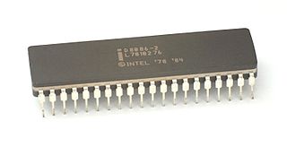
x86 is a family of complex instruction set computer (CISC) instruction set architectures initially developed by Intel based on the 8086 microprocessor and its 8088 variant. The 8086 was introduced in 1978 as a fully 16-bit extension of 8-bit Intel's 8080 microprocessor, with memory segmentation as a solution for addressing more memory than can be covered by a plain 16-bit address. The term "x86" came into being because the names of several successors to Intel's 8086 processor end in "86", including the 80186, 80286, 80386 and 80486. Colloquially, their names were "186", "286", "386" and "486".

Tejas was a code name for Intel's microprocessor, which was to be a successor to the latest Pentium 4 with the Prescott core and was sometimes referred to as Pentium V. Jayhawk was a code name for its Xeon counterpart. The cancellation of the processors in May 2004 underscored Intel's historical transition of its focus on single-core processors to multi-core processors.

x86-64 64-bit version of x86 architecture

x86-64 is a 64-bit version of the x86 instruction set, first announced in 1999. It introduced two new modes of operation, 64-bit mode and compatibility mode, along with a new 4-level paging mode.

<span class="mw-page-title-main">Xeon</span> Line of Intel server and workstation processors

Xeon is a brand of x86 microprocessors designed, manufactured, and marketed by Intel, targeted at the non-consumer workstation, server, and embedded markets. It was introduced in June 1998. Xeon processors are based on the same architecture as regular desktop-grade CPUs, but have advanced features such as support for error correction code (ECC) memory, higher core counts, more PCI Express lanes, support for larger amounts of RAM, larger cache memory and extra provision for enterprise-grade reliability, availability and serviceability (RAS) features responsible for handling hardware exceptions through the Machine Check Architecture (MCA). They are often capable of safely continuing execution where a normal processor cannot due to these extra RAS features, depending on the type and severity of the machine-check exception (MCE). Some also support multi-socket systems with two, four, or eight sockets through use of the Ultra Path Interconnect (UPI) bus, which replaced the older QuickPath Interconnect (QPI) bus.

<span class="mw-page-title-main">Multi-core processor</span> Microprocessor with more than one processing unit

A multi-core processor is a microprocessor on a single integrated circuit with two or more separate processing units, called cores, each of which reads and executes program instructions. The instructions are ordinary CPU instructions but the single processor can run instructions on separate cores at the same time, increasing overall speed for programs that support multithreading or other parallel computing techniques. Manufacturers typically integrate the cores onto a single integrated circuit die or onto multiple dies in a single chip package. The microprocessors currently used in almost all personal computers are multi-core.

<span class="mw-page-title-main">Pentium</span> Brand of discontinued microprocessors produced by Intel

Pentium is a discontinued series of x86 architecture-compatible microprocessors produced by Intel. The original Pentium was first released on March 22, 1993. The name "Pentium" is originally derived from the Greek word pente (πεντε), meaning "five", a reference to the prior numeric naming convention of Intel's 80x86 processors (8086–80486), with the Latin ending -ium since the processor would otherwise have been named 80586 using that convention.

<span class="mw-page-title-main">Larrabee (microarchitecture)</span> Canceled Intel GPGPU chip

Larrabee is the codename for a cancelled GPGPU chip that Intel was developing separately from its current line of integrated graphics accelerators. It is named after either Mount Larrabee or Larrabee State Park in Whatcom County, Washington, near the town of Bellingham. The chip was to be released in 2010 as the core of a consumer 3D graphics card, but these plans were cancelled due to delays and disappointing early performance figures. The project to produce a GPU retail product directly from the Larrabee research project was terminated in May 2010 and its technology was passed on to the Xeon Phi. The Intel MIC multiprocessor architecture announced in 2010 inherited many design elements from the Larrabee project, but does not function as a graphics processing unit; the product is intended as a co-processor for high performance computing.

<span class="mw-page-title-main">Dell Precision</span> Series of computer workstations

Dell Precision is a series of computer workstations for computer-aided design/architecture/computer graphics professionals, or as small-scale business servers. They are available in both desktop (tower) and mobile (laptop) form. Dell touts their Precision Mobile Workstations are "optimized for performance, reliability and user experience."

Tick–tock was a production model adopted in 2007 by chip manufacturer Intel. Under this model, every microarchitecture change (tock) was followed by a die shrink of the process technology (tick). It was replaced by the process–architecture–optimization model, which was announced in 2016 and is like a tick–tock cycle followed by an optimization phase. As a general engineering model, tick–tock is a model that refreshes one side of a binary system each release cycle.

Advanced Vector Extensions are SIMD extensions to the x86 instruction set architecture for microprocessors from Intel and Advanced Micro Devices (AMD). They were proposed by Intel in March 2008 and first supported by Intel with the Sandy Bridge processor shipping in Q1 2011 and later by AMD with the Bulldozer processor shipping in Q3 2011. AVX provides new features, new instructions, and a new coding scheme.

<span class="mw-page-title-main">Irish Centre for High-End Computing</span> National high-performance computing centre in Ireland

The Irish Centre for High-End Computing (ICHEC) is the national high-performance computing centre in Ireland. It was established in 2005 and provides supercomputing resources, support, training and related services. ICHEC is involved in education and training, including providing courses for researchers.

An AES instruction set is a set of instructions that are specifically designed to perform AES encryption and decryption operations efficiently. These instructions are typically found in modern processors and can greatly accelerate AES operations compared to software implementations. An AES instruction set includes instructions for key expansion, encryption, and decryption using various key sizes.

<span class="mw-page-title-main">LGA 2011</span> CPU socket created by Intel

LGA 2011, also called Socket R, is a CPU socket by Intel released on November 14, 2011. It launched along with LGA 1356 to replace its predecessor, LGA 1366 and LGA 1567. While LGA 1356 was designed for dual-processor or low-end servers, LGA 2011 was designed for high-end desktops and high-performance servers. The socket has 2011 protruding pins that touch contact points on the underside of the processor.

<span class="mw-page-title-main">Skylake (microarchitecture)</span> CPU microarchitecture by Intel

Skylake is Intel's codename for its sixth generation Core microprocessor family that was launched on August 5, 2015, succeeding the Broadwell microarchitecture. Skylake is a microarchitecture redesign using the same 14 nm manufacturing process technology as its predecessor, serving as a tock in Intel's tick–tock manufacturing and design model. According to Intel, the redesign brings greater CPU and GPU performance and reduced power consumption. Skylake CPUs share their microarchitecture with Kaby Lake, Coffee Lake, Whiskey Lake, and Comet Lake CPUs.

In computer architecture, 512-bit integers, memory addresses, or other data units are those that are 512 bits wide. Also, 512-bit central processing unit (CPU) and arithmetic logic unit (ALU) architectures are those that are based on registers, address buses, or data buses of that size. There are currently no mainstream general-purpose processors built to operate on 512-bit integers or addresses, though a number of processors do operate on 512-bit data.

<span class="mw-page-title-main">Silvermont</span> Microarchitecture from Intel

Silvermont is a microarchitecture for low-power Atom, Celeron and Pentium branded processors used in systems on a chip (SoCs) made by Intel. Silvermont forms the basis for a total of four SoC families:

AVX-512 are 512-bit extensions to the 256-bit Advanced Vector Extensions SIMD instructions for x86 instruction set architecture (ISA) proposed by Intel in July 2013, and first implemented in the 2016 Intel Xeon Phi x200, and then later in a number of AMD and other Intel CPUs. AVX-512 consists of multiple extensions that may be implemented independently. This policy is a departure from the historical requirement of implementing the entire instruction block. Only the core extension AVX-512F is required by all AVX-512 implementations.

References

  1. Ian Cutress & Anton Shilov (7 May 2019). "The Larrabee Chapter Closes: Intel's Final Xeon Phi Processors Now in EOL" . Retrieved 12 March 2020.
  2. "Intel® Xeon Phi™ Coprocessor System Software Developers Guide" (PDF). Intel. 8 November 2012. p. 16. Archived (PDF) from the original on 21 April 2024. Retrieved 1 May 2024.
  3. 1 2 Radek (18 June 2012). "Chip Shot: Intel Names the Technology to Revolutionize the Future of HPC - Intel Xeon Phi Product Family". Intel. Retrieved 12 December 2012.
  4. robert-reed (4 February 2013). "Best Known Methods for Using OpenMP on Intel Many Integrated Core (Intel MIC) Architecture". software.intel.com.
  5. Jeffers, James; Reinders, James (1 March 2013). Intel Xeon Phi Coprocessor High Performance Programming. Morgan Kaufmann. ISBN   978-0124104143.
  6. Hruska, Joel (8 May 2019). "Intel Quietly Kills Off Xeon Phi". ExtremeTech .
  7. "Intel scraps graphics chip based on Larrabee". Reuters . 6 December 2009.
  8. Sodani, Avinash; et al. (2016). "Knights Landing: Second-Generation Intel Xeon Phi Product". IEEE Micro . 36 (2): 34–46. doi:10.1109/MM.2016.25. S2CID   28837176.
  9. 1 2 "TOP500 - June 2013". TOP500. Retrieved 18 June 2013.
  10. "June 2023 | TOP500 Supercomputer Sites". www.top500.org.
  11. 1 2 "Intel Powers the World's Fastest Supercomputer, Reveals New and Future High Performance Computing Technologies" . Retrieved 21 June 2013.
  12. W1zzard (24 July 2018). "Intel is Giving up on Xeon Phi - Eight More Models Declared End-Of-Life". TechPowerUp.{{cite web}}: CS1 maint: numeric names: authors list (link)
  13. Marc Sauter (20 June 2016). "Knights Landing: Intel veröffentlicht Xeon Phi mit bis zu 7 Teraflops - Golem.de". www.golem.de (in German).
  14. Charlie Demerjian (3 July 2006), "New from Intel: It's Mini-Cores!", theinquirer.net, The Inquirer, archived from the original on 29 August 2009{{citation}}: CS1 maint: unfit URL (link)
  15. Seiler, L.; Cavin, D.; Espasa, E.; Grochowski, T.; Juan, M.; Hanrahan, P.; Carmean, S.; Sprangle, A.; Forsyth, J.; Abrash, R.; Dubey, R.; Junkins, E.; Lake, T.; Sugerman, P. (August 2008). "Larrabee: A Many-Core x86 Architecture for Visual Computing" (PDF). ACM Transactions on Graphics . Proceedings of ACM SIGGRAPH 2008. 27 (3): 18:11. doi:10.1145/1360612.1360617. ISSN   0730-0301. S2CID   52799248. Archived from the original (PDF) on 10 September 2015. Retrieved 6 August 2008.
  16. Tom Forsyth, SIMD Programming with Larrabee (PDF), Intel
  17. Ryan Smith (25 May 2010), "Intel Kills Larrabee GPU, Will Not Bring a Discrete Graphics Product to Market\", www.anandtech.com, AnandTech
  18. Tony Bradley (3 December 2009), "Intel 48-Core "Single-Chip Cloud Computer" Improves Power Efficiency", pcworld.com, PCWorld
  19. "Intel Research : Single-Chip Cloud Computer", techresearch.intel.com, Intel
  20. Ben Ames (11 February 2007), "Intel Tests Chip Design With 80-Core Processor", pcworld.com, IDG News, archived from the original on 17 January 2012, retrieved 14 November 2018
  21. "Intel Details 80-Core Teraflops Research Chip - X-bit labs". xbitlabs.com. Archived from the original on 5 February 2015. Retrieved 27 August 2015.
  22. "Intel's Teraflops Research Chip" (PDF), download.intel.com, Intel, archived from the original (PDF) on 16 May 2021
  23. Anton Shilov (12 February 2007), "Intel Details 80-Core Teraflops Research Chip", xbitlabs.com, Xbit laboratories, archived from the original on 5 February 2015
  24. 1 2 Rupert Goodwins (1 June 2010), "Intel unveils many-core Knights platform for HPC", zdnet.co.uk, ZDNet
  25. "Intel News Release : Intel Unveils New Product Plans for High-Performance Computing", intel.com, Intel, 31 May 2010
  26. 1 2 Mike Giles (24 June 2010), "Runners and riders in GPU steeplechase" (PDF), people.maths.ox.ac.uk, pp. 8–10
  27. 1 2 3 4 Gareth Halfacree (20 June 2011), "Intel pushes for HPC space with Knights Corner", thinq.co.uk, Net Communities Limited, UK
  28. "Intel Many Integrated Core Architecture" (PDF), many-core.group.cam.ac.uk, Intel, December 2010, archived from the original (PDF) on 2 April 2012
  29. Rick Merritt (20 June 2011), "OEMs show systems with Intel MIC chips", EE Times
  30. Tom R. Halfhill (18 July 2011), "Intel Shows MIC Progress", linleygroup.com, The Linley Group
  31. Andrea Petrou (20 June 2011), "SGI wants Intel for super supercomputer", news.techeye.net, archived from the original on 16 September 2011
  32. ""Stampede's" Comprehensive Capabilities to Bolster U.S. Open Science Computational Resources" (Press release). Texas Advanced Computing Center. 22 September 2011. Archived from the original on 5 August 2012. Retrieved 23 September 2011.
  33. 1 2 "Stampede: A Comprehensive Petascale Computing Environment" (PDF). IEEE Cluster 2011 Special Topic. Archived from the original (PDF) on 26 September 2012. Retrieved 16 November 2011.
  34. Yam, Marcus (16 November 2011), "Intel's Knights Corner: 50+ Core 22nm Co-processor", tomshardware.com, Tom's Hardware , retrieved 16 November 2011
  35. Sylvie Barak (16 November 2011), "Intel unveils 1 TFLOP/s Knights Corner", EE Times , retrieved 16 November 2011
  36. James Reinders (5 June 2012), Knights Corner: Open source software stack, Intel
  37. Prickett Morgan, Timothy (18 June 2012), "Intel slaps Xeon Phi brand on MIC coprocessors", 222.theregister.co.uk
  38. Intel Corporation (18 June 2012), "Latest Intel Xeon Processors E5 Product Family Achieves Fastest Adoption of New Technology on Top500 List", marketwatch.com, archived from the original on 20 June 2012, retrieved 18 June 2012, Intel Xeon Phi is the new brand name for all future Intel Many Integrated Core Architecture based products targeted at HPC, enterprise, datacenters and workstations. The first Intel Xeon Phi product family member is scheduled for volume production by the end of 2012
  39. Raj Hazra (18 June 2012). "Intel Xeon Phi coprocessors accelerate the pace of discovery and innovation". Intel. Retrieved 12 December 2012.
  40. Rick Merritt (18 June 2012). "Cray will use Intel MIC, branded Xeon Phi". EETimes. Retrieved 12 December 2012.
  41. Terrence O'Brien (18 June 2012). "Intel christens its 'Many Integrated Core' products Xeon Phi, eyes exascale milestone". Engadget. Retrieved 12 December 2012.
  42. Jeffrey Burt (18 June 2012). "Intel Wraps Xeon Phi Branding Around MIC Coprocessors". eWeek . Retrieved 7 March 2022.
  43. Merritt, Rick (8 June 2012), "Cray will use Intel MIC, branded Xeon Phi", eetimes.com
  44. Latif, Lawrence (19 June 2012), "Cray to support Intel's Xeon Phi in Cascade clusters", theinquirer.net, archived from the original on 22 June 2012{{citation}}: CS1 maint: unfit URL (link)
  45. "ScaleMP vSMP Foundation to Support Intel Xeon Phi" (Press release). ScaleMP. 20 June 2012. Archived from the original on 20 May 2013.
  46. George Chrysos (12 November 2012). "Intel Xeon Phi X100 Family Coprocessor - the Architecture". software.intel.com.
  47. 1 2 3 IntelPR (12 November 2012). "Intel Delivers New Architecture for Discovery with Intel Xeon Phi Coprocessors". Intel. Retrieved 12 December 2012.
  48. 1 2 3 Agam Shah (12 November 2012). "Intel ships 60-core Xeon Phi processor". Computerworld. Archived from the original on 12 March 2013. Retrieved 12 December 2012.
  49. 1 2 3 Johan De Gelas (14 November 2012). "The Xeon Phi at work at TACC". AnandTech. Retrieved 12 December 2012.
  50. "Tianhe-2 (MilkyWay-2)". Top500.org. 14 November 2015. Retrieved 6 May 2016.
  51. Hruska, Joel (30 July 2012). "Intel's 50-core champion: In-depth on Xeon Phi". ExtremeTech. Ziff Davis, Inc. Retrieved 2 December 2012.
  52. Barker, J; Bowden, J (2013). "Manycore Parallelism through OpenMP". OpenMP in the Era of Low Power Devices and Accelerators. IWOMP. Lecture Notes in Computer Science, vol 8122. Vol. 8122. Springer. pp. 45–57. doi:10.1007/978-3-642-40698-0_4. ISBN   978-3-642-40697-3.
  53. Rick Merritt (20 June 2011), "OEMs show systems with Intel MIC chips", EE Times
  54. Dokulil, Jiri; Bajrovic, Enes; Benkner, Siegfried; Pllana, Sabri; Sandrieser, Martin; Bachmayer, Beverly (23 November 2012), Efficient Hybrid Execution of C++ Applications using Intel Xeon Phi Coprocessor, arXiv: 1211.5530 , Bibcode:2012arXiv1211.5530D
  55. "News Fact Sheet: Intel Many Integrated Core (Intel MIC) Architecture ISC'11 Demos and Performance Description" (PDF), newsroom.intel.com, Intel, 20 June 2011, archived from the original (PDF) on 24 March 2012
  56. Tesla vs. Xeon Phi vs. Radeon. A Compiler Writer’s Perspective // The Portland Group (PGI), CUG 2013 Proceedings
  57. "Intel Many Integrated Core Architecture (Intel MIC Architecture) - RESOURCES (including downloads)". Intel. Retrieved 6 January 2014.
  58. "Intel Xeon Phi Coprocessor Instruction Set Architecture Reference Manual" (PDF). Intel. 7 September 2012. Retrieved 6 January 2014.
  59. "Intel Developer Zone: Intel Xeon Phi Coprocessor". Intel. Archived from the original on 1 February 2014. Retrieved 6 January 2014.
  60. "Intel® Intrinsics Guide". software.intel.com. Retrieved 4 August 2020.
  61. "Intel SE3110X Xeon Phi 3110X Knights Corner 6GB Coprocessor-No Cooling -SabrePC.com -SabrePC.com". www.sabrepc.com. Archived from the original on 22 February 2017. Retrieved 22 February 2017.
  62. "Intel Xeon Phi Coprocessor 3120A (6GB, 1.100 GHz, 57 core) Product Specifications". Intel ARK (Product Specs). Retrieved 22 February 2017.
  63. "Intel Xeon Phi Coprocessor 3120P (6GB, 1.100 GHz, 57 core) Product Specifications". Intel ARK (Product Specs). Retrieved 22 February 2017.
  64. "Intel Xeon Phi 31S1P - BC31S1P". www.cpu-world.com. Retrieved 21 April 2024.
  65. "Intel Xeon Phi Coprocessor 5110P (8GB, 1.053 GHz, 60 core) Product Specifications". Intel ARK (Product Specs). Retrieved 22 February 2017.
  66. "Intel Xeon Phi Coprocessor 5120D (8GB, 1.053 GHz, 60 core) Product Specifications". Intel ARK (Product Specs). Retrieved 22 February 2017.
  67. "Intel Xeon Phi SE10P". www.cpu-world.com. Retrieved 21 April 2024.
  68. "Intel Xeon Phi SE10X". www.cpu-world.com. Retrieved 21 April 2024.
  69. "Intel SC7110P Xeon Phi 7110P Knights Corner Coprocessor -SabrePC.com -SabrePC.com". www.sabrepc.com. Retrieved 22 February 2017.
  70. "Intel SC7110X Xeon Phi 7110X Knights Corner Coprocessor -SabrePC.com -SabrePC.com". www.sabrepc.com. Retrieved 22 February 2017.
  71. "Intel Xeon Phi Coprocessor 7120A (16GB, 1.238 GHz, 61 core) Product Specifications". Intel ARK (Product Specs). Retrieved 22 February 2017.
  72. "Intel Xeon Phi Coprocessor 7120D (16GB, 1.238 GHz, 61 core) Product Specifications". Intel ARK (Product Specs). Retrieved 22 February 2017.
  73. "Intel Xeon Phi Coprocessor 7120P (16GB, 1.238 GHz, 61 core) Product Specifications". Intel ARK (Product Specs). Retrieved 22 February 2017.
  74. "Intel Xeon Phi Coprocessor 7120X (16GB, 1.238 GHz, 61 core) Product Specifications". Intel ARK (Product Specs). Retrieved 22 February 2017.
  75. "Intel Xeon Phi 'Knights Landing' Features Integrated Memory With 500 GB/s Bandwidth and DDR4 Memory Support - Architecture Detailed". WCCFtech. 25 November 2013. Retrieved 27 August 2015.
  76. Sebastian Anthony (26 November 2013), Intel unveils 72-core x86 Knights Landing CPU for exascale supercomputing, ExtremeTech
  77. Tom's Hardware: Intel Xeon Phi Knights Landing Now Shipping; Omni Path Update, Too. 20 June 2016
  78. James Reinders (23 July 2013), AVX-512 Instructions, Intel
  79. "Cori". www.nersc.gov. Archived from the original on 17 May 2019. Retrieved 14 November 2018.
  80. 1 2 "2016 ISC High Performance: Intel's Rajeeb Hazra Delivers Keynote Address". Vimeo.
  81. Pradeep Dubey (20 June 2016). "How Intel Xeon Phi Processors Benefit Machine Learning/Deep Learning Apps and Frameworks". software.intel.com.
  82. "Introducing the Intel Xeon Phi Processor – Your Path to Deeper Insight". Intel. Archived from the original on 27 January 2017.
  83. "TOP500_List November 2016".
  84. Larabel, Michael (24 August 2017). "Intel Quietly Drops Xeon Phi 7200 Coprocessors". Phoronix. Retrieved 25 August 2017.
  85. "Product Change Notification 116378 - 00" (PDF). Intel.com. Retrieved 25 July 2018.
  86. "Intel Xeon Phi processor: Your Path to Deeper Insight" (PDF). Intel.com. Archived from the original (PDF) on 26 February 2017. Retrieved 25 February 2017.
  87. "Intel Xeon Phi 7220A".
  88. "Intel Xeon Phi 7220P".
  89. "Intel Xeon Phi 7240P".
  90. "Intel Xeon Phi Processor 7210 (16GB, 1.30 GHz, 64 core) Product Specifications". Intel ARK (Product Specs). Retrieved 22 February 2017.
  91. "Intel Xeon Phi Processor 7210F (16GB, 1.30 GHz, 64 core) Product Specifications". Intel ARK (Product Specs). Retrieved 22 February 2017.
  92. "Intel Xeon Phi Processor 7230 (16GB, 1.30 GHz, 64 core) Product Specifications". Intel ARK (Product Specs). Retrieved 22 February 2017.
  93. "Intel Xeon Phi Processor 7230F (16GB, 1.30 GHz, 64 core) Product Specifications". Intel ARK (Product Specs). Retrieved 22 February 2017.
  94. "Intel Xeon Phi Processor 7250 (16GB, 1.40 GHz, 68 core) Product Specifications". Intel ARK (Product Specs). Retrieved 22 February 2017.
  95. "Intel Xeon Phi Processors". Intel. Retrieved 25 February 2017.
  96. "Intel Xeon Phi Processor 7250F (16GB, 1.40 GHz, 68 core) Product Specifications". Intel ARK (Product Specs). Retrieved 22 February 2017.
  97. "Intel Xeon Phi Processor 7290 (16GB, 1.50 GHz, 72 core) Product Specifications". Intel ARK (Product Specs). Retrieved 22 February 2017.
  98. "Intel Xeon Phi Processor 7290F (16GB, 1.50 GHz, 72 core) Product Specifications". Intel ARK (Product Specs). Retrieved 22 February 2017.
  99. Smith, Ryan (17 August 2016). "Intel Announces Knight's Mill: A Xeon Phi for Deep Learning". Anandtech. Retrieved 17 August 2016.
  100. Cutress, Ian (19 December 2017). "Intel Lists Knights Mill Xeon Phi on ARK: Up to 72 cores at 320W with QFMA and VNNI". Anandtech. Retrieved 19 December 2017.
  101. SC14: Supercomputing '14; International Conference for High Performance Computing, Networking, Storage and Analysis in year 2014
  102. Eric Gardner (25 November 2014), What public disclosures has Intel made about Knights Landing?, Intel Corporation, archived from the original on 23 February 2015
  103. ALCF staff (9 April 2015), Introducing Aurora
  104. ALCF staff (9 April 2015), Aurora
  105. Hemsoth, Nicole (23 May 2017). "Some Surprises in the 2018 DoE Budget for Supercomputing". Next Platform. Retrieved 13 November 2017.
  106. Brueckner, Rich (16 June 2017). "Is Aurora Morphing into an Exascale AI Supercomputer?". Inside HPC. Retrieved 13 November 2017.
  107. Damkroger, Trish (13 November 2017). "Unleashing high performance computing today and tomorrow". Intel IT Peer Network.
  108. Kampman, Jeff (13 November 2017). "Intel quietly kills off next-gen Knights Hill Xeon Phi chips". Tech Report. Retrieved 13 November 2017.
  109. Fang, Jianbin; Sips, Henk; Zhang, Lilun; Xu, Chuanfu; Yonggang, Che; Varbanescu, Ana Lucia (2014). Test-Driving Intel Xeon Phi (PDF). 2014 ACM/SPEC International Conference on Performance Engineering. Archived from the original (PDF) on 11 November 2017. Retrieved 30 December 2013.
  110. Memeti, Suejb; Pllana, Sabri; Benkner, Siegfried; Pllana, Sabri; Sandrieser, Martin; Bachmayer, Beverly (29 June 2015), Accelerating DNA Sequence Analysis using Intel Xeon Phi, arXiv: 1506.08612 , Bibcode:2015arXiv150608612M
  111. Viebke, Andre; Pllana, Sabri; Benkner, Siegfried; Pllana, Sabri; Sandrieser, Martin; Bachmayer, Beverly (30 June 2015), The Potential of the Intel Xeon Phi for Supervised Deep Learning, arXiv: 1506.09067 , Bibcode:2015arXiv150609067V
  112. Jon Stokes (20 June 2011). "Intel takes wraps off 50-core supercomputing processor plans". Ars Technica .
  113. 1 2 Johan De Gelas (11 September 2012). "Intel's Xeon Phi in 10 Petaflops supercomputer". AnandTech. Retrieved 12 December 2012.