Open NAND Flash Interface Working Group

Last updated
Open NAND Flash Interface Working Group
FormationMarch 2006
TypeIndustry trade group
Purpose Flash memory standardization
Website www.onfi.org

The Open NAND Flash Interface Working Group (ONFI or ONFi [1] with a lower case "i") is a consortium of technology companies working to develop open standards for NAND flash memory and devices that communicate with them. The formation of ONFI was announced at the Intel Developer Forum in March 2006. [2]

Contents

History

The group's goals did not include the development of a new consumer flash memory card format. [3] Rather, ONFI seeks to standardize the low-level interface to raw NAND flash chips, which are the most widely used form of non-volatile memory integrated circuits (chips); in 2006, nearly one trillion MiB of flash memory was incorporated into consumer electronics, and production was expected to double by 2007. [4] As of 2006, NAND flash memory chips from most vendors used similar packaging, had similar pinouts, and accepted similar sets of low-level commands. As a result, when more capable and inexpensive models of NAND flash become available, product designers can incorporate them without major design changes. However, "similar" operation is not optimal: [5] subtle differences in timing and command set mean that products must be thoroughly debugged and tested when a new model of flash chip is used in them. [4] When a flash controller is expected to operate with various NAND flash chips, it must store a table of them in its firmware so that it knows how to deal with differences in their interfaces. [4] [5] This increases the complexity and time-to-market of flash-based devices, and means they are likely to be incompatible with future models of NAND flash, unless and until their firmware is updated.

Thus, one of the main motivations for standardization of NAND flash was to make it easier to switch between NAND chips from different producers, thereby permitting faster development of NAND-based products and lower prices via increased competition among manufacturers. By 2006, NAND flash became increasingly a commodity product, [6] like SDRAM or hard disk drives. It is incorporated into many personal computer and consumer electronics products such as USB flash drives, MP3 players, and solid-state drives. Product designers wanted newer NAND flash chips, for example, to be as easily interchangeable as hard disks from different manufacturers. [6] [7]

Historical similarities

The effort to standardize NAND flash may be compared to earlier standardization of electronic components. For example, the 7400 series of TTL digital integrated circuits were originally produced by Texas Instruments, but had become a de facto standard family by the late 1970s. These ICs are manufactured as commodity parts by a number of different vendors. This has allowed designers to freely mix 7400 components from different vendorsand even to mix components based on different logic families, once the 74HCT sub-family become available (consisting of CMOS components with TTL-compatible logic levels).

Members

The ONFI consortium included manufacturers of NAND flash memory such as Hynix, Intel, Micron Technology, Phison, Western Digital, Sony and Spansion. [2] Samsung, the world's largest manufacturer of NAND flash, was absent in 2006. [8] Vendors of NAND flash-based consumer electronics and computing products are also members.

Specifications

ONFI produced specifications for standard interface to NAND flash chips.

Version 1.0 of this specification was released on December 28, 2006, and made available at no cost from the ONFI web site. Samsung was still not a participant. [9] It specified:

A verification product was announced in June 2009. [10]

Version 2.3 was published in August 2010. It included a protocol called EZ-NAND that hid ECC details. [11]

Version 3.0 was published in March 2011. It required fewer chip-enable pins enabling more efficient printed circuit board routing. [12] A standard developed jointly with the JEDEC was published in October 2012. [13] [14]

Version 3.1, published in october of 2012, includes errata to the original ONFI 3.0 specification, adds LUN SET/GET Features commands, and implements additional data setup and hold values for NV-DDR2 interface.

Version 3.2, published on July 23, 2013, raised the data rate to 533 MB/s. [15]

Version 4.0, published on April 17, 2014, introduced the NV-DDR3 interface increases the maximum switching speed from 533 MB/s to 800 MB/s, providing a performance boost of up to 50% for high performance applications enabled by solid-state NAND storage components. [16]

Version 4.1, published on December 12, 2017, extends NV-DDR3 I/O speeds to 1066 MT/s and 1200MT/s. [17]   For better signaling performance, ONFI 4.1 adds Duty Cycle Correction (DCC), Read and Write Training for speeds greater than 800MT/s, support for lower pin cap devices with 37.5 Ohms default output resistance, and devices which require data burst exit and restart for long data input and output pauses.  For lower power, 2.5V Vcc support is added. ONFI 4.1 also includes errata to the ONFI 4.0 specification.

Version 4.2, published on February 12, 2020, extends NV-DDR3 I/O speeds to 1333MT/s, 1466MT/s and 1600MT/s. The BGA-252b four channel package is introduced which has a smaller footprint than the existing BGA-272b four channel package. To enable higher IOPS multi-plane operations, addressing restrictions related to multi-plane operations are relaxed. [18]

Version 5.0, Published in May 2021, ONFI5.0 extends NV-DDR3 I/O speeds up to 2400MT/s. A new NV-LPDDR4 lower power interface is introduced with speeds up to 2400MT/s. With the NV-LPDDR4 interface, an optional Data Bus Inversion (DBI) feature is defined. New smaller footprint BGA-178b, BGA-154b and BGA-146b packages are added. ONFI5.0 also includes other errata related to the ONFI4.2 specification. [19]

Block Abstracted NAND

ONFI created the Block Abstracted NAND addendum specification to simplify host controller design by relieving the host of the complexities of ECC, bad block management, and other low-level NAND management tasks. The ONFI Block Abstracted NAND revision 1.1 specification adds the high speed source synchronous interface, which provides up to a 5X improvement in bandwidth compared with the traditional asynchronous NAND interface. [20]

NAND Connector

The NAND Connector Specification was ratified in April 2008. It specifies a standardized connection for NAND modules (similar to DRAM DIMMs) for use in applications like caching and solid-state drives (SSDs) in PC platforms.

See also

Related Research Articles

<span class="mw-page-title-main">DDR SDRAM</span> Type of computer memory

Double Data Rate Synchronous Dynamic Random-Access Memory is a double data rate (DDR) synchronous dynamic random-access memory (SDRAM) class of memory integrated circuits used in computers. DDR SDRAM, also retroactively called DDR1 SDRAM, has been superseded by DDR2 SDRAM, DDR3 SDRAM, DDR4 SDRAM and DDR5 SDRAM. None of its successors are forward or backward compatible with DDR1 SDRAM, meaning DDR2, DDR3, DDR4 and DDR5 memory modules will not work on DDR1-equipped motherboards, and vice versa.

<span class="mw-page-title-main">Flash memory</span> Electronic non-volatile computer storage device

Flash memory is an electronic non-volatile computer memory storage medium that can be electrically erased and reprogrammed. The two main types of flash memory, NOR flash and NAND flash, are named for the NOR and NAND logic gates. Both use the same cell design, consisting of floating gate MOSFETs. They differ at the circuit level depending on whether the state of the bit line or word lines is pulled high or low: in NAND flash, the relationship between the bit line and the word lines resembles a NAND gate; in NOR flash, it resembles a NOR gate.

<span class="mw-page-title-main">DIMM</span> Computer memory module

A DIMM, or Dual In-Line Memory Module, is a type of computer memory module used in desktop, laptop, and server computers. It is a circuit board that contains memory chips and connects to the computer's motherboard. A DIMM is often called a "RAM stick" due to its shape and size. A DIMM comprises a series of dynamic random-access memory integrated circuits that are mounted to its circuit board. DIMMs are the predominant method for adding memory into a computer system. The vast majority of DIMMs are standardized through JEDEC standards, although there are proprietary DIMMs. DIMMs come in a variety of speeds and sizes, but generally are one of two lengths - PC which are 133.35 mm (5.25 in) and laptop (SO-DIMM) which are about half the size at 67.60 mm (2.66 in).

<span class="mw-page-title-main">DDR2 SDRAM</span> Second generation of double-data-rate synchronous dynamic random-access memory

Double Data Rate 2 Synchronous Dynamic Random-Access Memory is a double data rate (DDR) synchronous dynamic random-access memory (SDRAM) interface. It is a JEDEC standard (JESD79-2); first published in September 2003. DDR2 succeeded the original DDR SDRAM specification, and was itself succeeded by DDR3 SDRAM in 2007. DDR2 DIMMs are neither forward compatible with DDR3 nor backward compatible with DDR.

<span class="mw-page-title-main">CompactFlash</span> Memory card format

CompactFlash (CF) is a flash memory mass storage device used mainly in portable electronic devices. The format was specified and the devices were first manufactured by SanDisk in 1994.

<span class="mw-page-title-main">MultiMediaCard</span> Memory card format

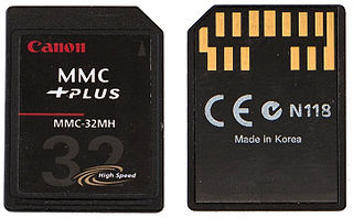
The MultiMediaCard, officially abbreviated as MMC, is a memory card standard used for solid-state storage. Unveiled in 1997 by SanDisk and Siemens, MMC is based on a surface-contact low pin-count serial interface using a single memory stack substrate assembly, and is therefore much smaller than earlier systems based on high pin-count parallel interfaces using traditional surface-mount assembly such as CompactFlash. Both products were initially introduced using SanDisk NOR-based flash technology.

The Common Flash Memory Interface (CFI) is an open standard jointly developed by AMD, Intel, Sharp and Fujitsu. It is implementable by all flash memory vendors, and has been approved by the non-volatile-memory subcommittee of JEDEC. The goal of the specification is the interchangeability of flash memory devices offered by different vendors. The developer is able to use one driver for different flash products by reading identifying information from the flash chip.

Double Data Rate 3 Synchronous Dynamic Random-Access Memory is a type of synchronous dynamic random-access memory (SDRAM) with a high bandwidth interface, and has been in use since 2007. It is the higher-speed successor to DDR and DDR2 and predecessor to DDR4 synchronous dynamic random-access memory (SDRAM) chips. DDR3 SDRAM is neither forward nor backward compatible with any earlier type of random-access memory (RAM) because of different signaling voltages, timings, and other factors.

<span class="mw-page-title-main">GDDR5 SDRAM</span> Type of high performance DRAM graphics card memory

Graphics Double Data Rate 5 Synchronous Dynamic Random-Access Memory is a type of synchronous graphics random-access memory (SGRAM) with a high bandwidth interface designed for use in graphics cards, game consoles, and high-performance computing. It is a type of GDDR SDRAM.

Package on a package (PoP) is an integrated circuit packaging method to vertically combine discrete logic and memory ball grid array (BGA) packages. Two or more packages are installed atop each other, i.e. stacked, with a standard interface to route signals between them. This allows higher component density in devices, such as mobile phones, personal digital assistants (PDA), and digital cameras, at the cost of slightly higher height requirements. Stacks with more than 2 packages are uncommon, due to heat dissipation considerations.

Universal Flash Storage (UFS) is a flash storage specification for digital cameras, mobile phones and consumer electronic devices. It was designed to bring higher data transfer speed and increased reliability to flash memory storage, while reducing market confusion and removing the need for different adapters for different types of cards. The standard encompasses both packages permanently attached (embedded) within a device (eUFS), and removable UFS memory cards.

<span class="mw-page-title-main">Vortex86</span> X86-compatible system-on-a-chip

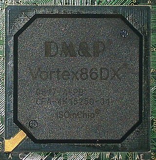
The Vortex86 is a computing system-on-a-chip (SoC) based on a core compatible with the x86 microprocessor family. It is produced by DM&P Electronics, but originated with Rise Technology.

Double Data Rate 4 Synchronous Dynamic Random-Access Memory is a type of synchronous dynamic random-access memory with a high bandwidth interface.

<span class="mw-page-title-main">UniPro</span>

UniPro is a high-speed interface technology for interconnecting integrated circuits in mobile and mobile-influenced electronics. The various versions of the UniPro protocol are created within the MIPI Alliance, an organization that defines specifications targeting mobile and mobile-influenced applications.

Everspin Technologies is a public semiconductor company headquartered in Chandler, Arizona, United States. It develops and manufactures discrete magnetoresistive RAM or magnetoresistive random-access memory (MRAM) products, including Toggle MRAM and Spin-Transfer Torque MRAM (STT-MRAM) product families. It also licenses its technology for use in embedded MRAM (eMRAM) applications, magnetic sensor applications as well as performs backend foundry services for eMRAM.

Hybrid Memory Cube (HMC) is a high-performance computer random-access memory (RAM) interface for through-silicon via (TSV)-based stacked DRAM memory. HMC competes with the incompatible rival interface High Bandwidth Memory (HBM).

A NVDIMM or non-volatile DIMM is a type of persistent random-access memory for computers using widely used DIMM form-factors. Non-volatile memory is memory that retains its contents even when electrical power is removed, for example from an unexpected power loss, system crash, or normal shutdown. Properly used, NVDIMMs can improve application performance and system crash recovery time. They enhance solid-state drive (SSD) endurance and reliability.

<span class="mw-page-title-main">DDR5 SDRAM</span> Fifth generation of double-data-rate synchronous dynamic random-access memory

Double Data Rate 5 Synchronous Dynamic Random-Access Memory is a type of synchronous dynamic random-access memory. Compared to its predecessor DDR4 SDRAM, DDR5 was planned to reduce power consumption, while doubling bandwidth. The standard, originally targeted for 2018, was released on July 14, 2020.

<span class="mw-page-title-main">UniDIMM</span> Specification for DIMMs

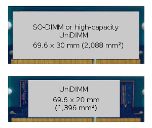
UniDIMM is a specification for dual in-line memory modules (DIMMs), which are printed circuit boards (PCBs) designed to carry dynamic random-access memory (DRAM) chips. UniDIMMs can be populated with either DDR3 or DDR4 chips, with no support for any additional memory control logic; as a result, the computer's memory controller must support both DDR3 and DDR4 memory standards. The UniDIMM specification was created by Intel for its Skylake microarchitecture, whose integrated memory controller (IMC) supports both DDR3 and DDR4 memory technologies.

<span class="mw-page-title-main">High Bandwidth Memory</span> Type of memory used on processors that require high transfer rate memory

High Bandwidth Memory (HBM) is a computer memory interface for 3D-stacked synchronous dynamic random-access memory (SDRAM) initially from Samsung, AMD and SK Hynix. It is used in conjunction with high-performance graphics accelerators, network devices, high-performance datacenter AI ASICs, as on-package cache in CPUs and on-package RAM in upcoming CPUs, and FPGAs and in some supercomputers. The first HBM memory chip was produced by SK Hynix in 2013, and the first devices to use HBM were the AMD Fiji GPUs in 2015.

References

  1. "ONFI web site presentation page". ONFI.org. Retrieved 2010-07-31.
  2. 1 2 "New Group Simplifies NAND Flash Integration". Press release. ONFI. May 9, 2006. Retrieved September 13, 2013.
  3. "ONFI FAQ page". ONFI.org. Retrieved 2010-07-31.
  4. 1 2 3 Huffman, Amber. "Open NAND Flash Interface: The First Wave of NAND Standardization" (PDF). ONFI.org. Archived from the original (PDF) on 2012-02-19. Retrieved 2010-07-31.
  5. 1 2 Kamat, Arun. "Simplifying Flash Controller Design" (PDF). ONFI.org. Archived from the original (PDF) on 2012-02-19. Retrieved 2010-07-31. See section "The Curse of Similarity" in this white paper by Arun Kamat of Hynix.
  6. 1 2 See this presentation by Amber Huffman and Michael Abraham of Micron.
  7. Jim Cooke (September 25, 2006). "Simplify Your Flash-Memory Interface". Dr. Dobb's Journal . Retrieved September 13, 2013.
  8. Tony Smith (May 11, 2006). "Intel primes Flash standardisation push: Industry body formed to define common interface". The Register . Retrieved September 13, 2013.
  9. Tony Smith (January 22, 2007). "Vendors pledge to make Flash as easy to upgrade as RAM: Open Flash spec published". The Register. Retrieved September 13, 2013.
  10. "Perfectus Announces Industry's First SystemVerilog-based OVM Tested ONFi Verification IP for ONFi 2.1 Specification". Press release. June 22, 2009. Retrieved September 13, 2013.
  11. Mark LaPedus (August 16, 2010). "NAND specification adds error correction". EE Times. Retrieved September 13, 2013.
  12. "ONFI specification version 3.0" (PDF). March 15, 2011. Retrieved September 13, 2013.
  13. "JEDEC and the Open NAND Flash Interface Workgroup Publish NAND Flash Interface Interoperability Standard". Press release. JEDEC. November 6, 2012. Retrieved September 13, 2013.
  14. "NAND Flash Interface Interoperability: JEDSD230" (PDF). October 30, 2012. Retrieved September 13, 2013.
  15. "ONFI Announces Publication of 3.2 Standard, Pushes Data Transfer Speeds to 533 MB/sec". Press release. ONFI. July 23, 2013. Retrieved September 13, 2013.
  16. "ONFI Announces Publication of 4.0 Standard, Enabling a New Generation I/O with Lower Power and Higher Bandwidth". Press release. ONFI. April 17, 2014.
  17. "Specifications - ONFi". www.onfi.org. Retrieved 2018-09-18.
  18. "Open NAND Flash Interface Specification Revision 4.2" (PDF). 2020-02-12.
  19. "Open NAND Flash Interface Specification Revision 5.0" (PDF). 25 May 2021.
  20. "Block Abstracted NAND specification version 1.1" (PDF). July 8, 2009. Retrieved September 13, 2013.