Related Research Articles

MEMS is the technology of microscopic devices incorporating both electronic and moving parts. MEMS are made up of components between 1 and 100 micrometres in size, and MEMS devices generally range in size from 20 micrometres to a millimetre, although components arranged in arrays can be more than 1000 mm2. They usually consist of a central unit that processes data and several components that interact with the surroundings.
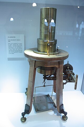
Piezoelectricity is the electric charge that accumulates in certain solid materials—such as crystals, certain ceramics, and biological matter such as bone, DNA, and various proteins—in response to applied mechanical stress. The word piezoelectricity means electricity resulting from pressure and latent heat. It is derived from Ancient Greek πιέζω (piézō) 'to squeeze or press', and ἤλεκτρον (ḗlektron) 'amber'.
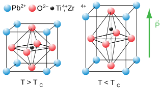
Lead zirconate titanate, also called lead zirconium titanate and commonly abbreviated as PZT, is an inorganic compound with the chemical formula Pb[ZrxTi1−x]O3(0 ≤ x ≤ 1). It is a ceramic perovskite material that shows a marked piezoelectric effect, meaning that the compound changes shape when an electric field is applied. It is used in a number of practical applications such as ultrasonic transducers and piezoelectric resonators. It is a white to off-white solid.
Energy harvesting is the process by which energy is derived from external sources, then stored for use by small, wireless autonomous devices, like those used in wearable electronics, condition monitoring, and wireless sensor networks.

A piezoelectric sensor is a device that uses the piezoelectric effect to measure changes in pressure, acceleration, temperature, strain, or force by converting them to an electrical charge. The prefix piezo- is Greek for 'press' or 'squeeze'.
A thin-film bulk acoustic resonator is a device consisting of a piezoelectric material manufactured by thin film methods between two conductive – typically metallic – electrodes and acoustically isolated from the surrounding medium. The operation is based on the piezoelectricity of the piezolayer between the electrodes.

Deformable mirrors (DM) are mirrors whose surface can be deformed, in order to achieve wavefront control and correction of optical aberrations. Deformable mirrors are used in combination with wavefront sensors and real-time control systems in adaptive optics. In 2006 they found a new use in femtosecond pulse shaping.
Micropower describes the use of very small electric generators and prime movers or devices to convert heat or motion to electricity, for use close to the generator. The generator is typically integrated with microelectronic devices and produces "several watts of power or less." These devices offer the promise of a power source for portable electronic devices which is lighter weight and has a longer operating time than batteries.
A MEMS thermal actuator is a microelectromechanical device that typically generates motion by thermal expansion amplification. A small amount of thermal expansion of one part of the device translates to a large amount of deflection of the overall device. Usually fabricated out of doped single crystal silicon or polysilicon as a complex compliant member, the increase in temperature can be achieved internally by electrical resistive heating or by a heat source capable of locally introducing heat. Microfabricated thermal actuators can be integrated into micromotors.

A radio-frequency microelectromechanical system is a microelectromechanical system with electronic components comprising moving sub-millimeter-sized parts that provide radio-frequency (RF) functionality. RF functionality can be implemented using a variety of RF technologies. Besides RF MEMS technology, III-V compound semiconductor, ferrite, ferroelectric, silicon-based semiconductor, and vacuum tube technology are available to the RF designer. Each of the RF technologies offers a distinct trade-off between cost, frequency, gain, large-scale integration, lifetime, linearity, noise figure, packaging, power handling, power consumption, reliability, ruggedness, size, supply voltage, switching time and weight.

Micropumps are devices that can control and manipulate small fluid volumes. Although any kind of small pump is often referred to as micropump, a more accurate definition restricts this term to pumps with functional dimensions in the micrometer range. Such pumps are of special interest in microfluidic research, and have become available for industrial product integration in recent years. Their miniaturized overall size, potential cost and improved dosing accuracy compared to existing miniature pumps fuel the growing interest for this innovative kind of pump.

A MEMSmagnetic field sensor is a small-scale microelectromechanical systems (MEMS) device for detecting and measuring magnetic fields (Magnetometer). Many of these operate by detecting effects of the Lorentz force: a change in voltage or resonant frequency may be measured electronically, or a mechanical displacement may be measured optically. Compensation for temperature effects is necessary. Its use as a miniaturized compass may be one such simple example application.
A MEMS magnetic actuator is a device that uses the microelectromechanical systems (MEMS) to convert an electric current into a mechanical output by employing the well-known Lorentz Force Equation or the theory of Magnetism.
Microelectromechanical system oscillators are devices that generate highly stable reference frequencies to measure time. The core technologies used in MEMS oscillators have been in development since the mid-1960s, but have only been sufficiently advanced for commercial applications since 2006. MEMS oscillators incorporate MEMS resonators, which are microelectromechanical structures that define stable frequencies. MEMS clock generators are MEMS timing devices with multiple outputs for systems that need more than a single reference frequency. MEMS oscillators are a valid alternative to older, more established quartz crystal oscillators, offering better resilience against vibration and mechanical shock, and reliability with respect to temperature variation.

A microscanner, or micro scanning mirror, is a microoptoelectromechanical system (MOEMS) in the category of micromirror actuators for dynamic light modulation. Depending upon the type of microscanner, the modulatory movement of a single mirror can be either translatory or rotational, on one or two axes. In the first case, a phase shifting effect takes place. In the second case, the incident light wave is deflected.
Piezoelectric Micromachined Ultrasonic Transducers (PMUT) are MEMS-based piezoelectric ultrasonic transducers. Unlike bulk piezoelectric transducers which use the thickness-mode motion of a plate of piezoelectric ceramic such as PZT or single-crystal PMN-PT, PMUT are based on the flexural motion of a thin membrane coupled with a thin piezoelectric film, such as PVDF. In comparison with bulk piezoelectric ultrasound transducers, PMUT can offer advantages such as increased bandwidth, flexible geometries, natural acoustic impedance match with water, reduced voltage requirements, mixing of different resonant frequencies and potential for integration with supporting electronic circuits especially for miniaturized high frequency applications.

Richard Stephen Muller is an American professor in the Electrical Engineering and Computer Science Department of the University of California at Berkeley.
A nanoelectromechanical (NEM) relay is an electrically actuatedswitch that is built on the nanometer scale using semiconductor fabrication techniques. They are designed to operate in replacement of, or in conjunction with, traditional semiconductor logic. While the mechanical nature of NEM relays makes them switch much slower than solid-state relays, they have many advantageous properties, such as zero current leakage and low power consumption, which make them potentially useful in next generation computing.
Inkjet technology originally was invented for depositing aqueous inks on paper in 'selective' positions based on the ink properties only. Inkjet nozzles and inks were designed together and the inkjet performance was based on a design. It was used as a data recorder in the early 1950s, later in the 1950s co-solvent-based inks in the publishing industry were seen for text and images, then solvent-based inks appeared in industrial marking on specialized surfaces and in the1990's phase change or hot-melt ink has become a popular with images and digital fabrication of electronic and mechanical devices, especially jewelry. Although the terms "jetting", "inkjet technology" and "inkjet printing", are commonly used interchangeably, inkjet printing usually refers to the publishing industry, used for printing graphical content, while industrial jetting usually refers to general purpose fabrication via material particle deposition.
References
- ↑ "High-Speed Switching Enhances Piezoelectric Response in piezoMEMS Devices". AZoSensors. August 30, 2017. Retrieved August 27, 2018.
- ↑ "PZT". SINTEF. April 22, 2010. Retrieved August 27, 2018.
- 1 2 Polcawich, Ronald; Judy, Daniel; Pulskamp, Jeffrey; Trolier-McKinstry, Susan; Dubey, Madan (June 2007). "Advances in Piezoelectrically Actuated RF MEMS Switches and Phase Shifters". 2007 IEEE/MTT-S International Microwave Symposium: 2083–2086. doi:10.1109/MWSYM.2007.380297. ISBN 978-1-4244-0687-6. ISSN 0149-645X. S2CID 19897747.
- 1 2 3 Metzger, Brian. "Piezoelectric MEMS (PiezoMEMS) Patent Portfolio: Thin Film PZT Deposition, Development, Device Designs, and Testing". TechLink. Retrieved August 27, 2018.
- ↑ Polcawich, Ronald; Pulskamp, Jeffrey; Judy, Daniel; Ranade, Prashant; Trolier-McKinstry, Susan; Dubey, Madan (December 6, 2007). "Surface Micromachined Microelectromechancial Ohmic Series Switch Using Thin-Film Piezoelectric Actuators". IEEE Transactions on Microwave Theory and Techniques. 55 (12): 2642–2654. Bibcode:2007ITMTT..55.2642P. doi:10.1109/TMTT.2007.910072. S2CID 15283027.
- 1 2 Eom, Chang-Beom; Trolier-McKinstry, Susan (November 2012). "Thin-film piezoelectric MEMS". MRS Bulletin. 37 (11): 1007–1017. doi:10.1557/mrs.2012.273. S2CID 110494049.
- ↑ Lee, Hee-Chul; Park, Jae-Yeong; Bu, Jong-Uk (April 11, 2005). "Piezoelectrically actuated RF MEMS DC contact switches with low voltage operation". IEEE Microwave and Wireless Components Letters. 15 (4): 202–204. doi:10.1109/LMWC.2005.845689.
- 1 2 "Army Research Laboratory (ARL) Scientist Honored as the Department of Defense (DoD) Laboratory Scientist of the Quarter". Department of Defense Research & Engineering Enterprise. Retrieved August 27, 2018.
- ↑ Brewer, Steven; Cress, Cory; Williams, Samuel; Zhou, Hanhan; Rivas, Manuel; Polcawich, Ronald; Glaser, Evan; Jones, Jacob; Bassiri-Gharb, Nazanin (July 13, 2017). "Phenomenological Model for Defect Interactions in Irradiated Functional Materials". Scientific Reports. 7 (1): 5308. Bibcode:2017NatSR...7.5308B. doi:10.1038/s41598-017-05071-z. PMC 5509665 . PMID 28706227.
- ↑ Polcawich, Ronald (November 2004). "A Piezoelectric MEMS Microphone Based on Lead Zirconate Titanate (PZT) Thin Films". U.S. Army Research Laboratory. Archived from the original on June 3, 2018 – via Defense Technical Information Center.
- ↑ Polcawich, Ronald; Pulskamp, Jeffrey; Judy, Daniel; Ranade, Prashant; Trolier-McKinstry, Susan; Dubey, Madan (December 6, 2007). "Surface Micromachined Microelectromechancial Ohmic Series Switch Using Thin-Film Piezoelectric Actuators". IEEE Transactions on Microwave Theory and Techniques. 55 (12): 2642–2654. Bibcode:2007ITMTT..55.2642P. doi:10.1109/TMTT.2007.910072. S2CID 15283027.
- ↑ Pulskamp, Jeffrey; Judy, Daniel; Polcawish, Ronald; Kaul, Roger; Chandrahalim, Hengky; Bhave, Sunil (January 2009). Monolithically Integrated Piezomems SP2T Switch and Contour-Mode Filters. 2009 IEEE 22nd International Conference on Micro Electro Mechanical Systems. pp. 900–903. CiteSeerX 10.1.1.162.2655 . doi:10.1109/MEMSYS.2009.4805529. ISBN 978-1-4244-2977-6. S2CID 18225031.
- ↑ Pulskamp, Jeffrey (February 2005). "Modeling, Fabrication, and Testing of a Piezoelectric MEMS Vibrational Energy Reclamation Device". U.S. Army Research Laboratory. Archived from the original on June 1, 2018 – via Defense Technical Information Center.
- 1 2 Tadigadapa, Srinivas (September 2010). "Piezoelectric microelectromechanical systems — challenges and opportunities". Procedia Engineering. 5: 468–471. doi: 10.1016/j.proeng.2010.09.148 .