Register-transfer level

Last updated

In digital circuit design, register-transfer level (RTL) is a design abstraction which models a synchronous digital circuit in terms of the flow of digital signals (data) between hardware registers, and the logical operations performed on those signals.

Contents

Register-transfer-level abstraction is used in hardware description languages (HDLs) like Verilog and VHDL to create high-level representations of a circuit, from which lower-level representations and ultimately actual wiring can be derived. Design at the RTL level is typical practice in modern digital design. [1]

Unlike in software compiler design, where the register-transfer level is an intermediate representation and at the lowest level, the RTL level is the usual input that circuit designers operate on. In fact, in circuit synthesis, an intermediate language between the input register transfer level representation and the target netlist is sometimes used. Unlike in netlist, constructs such as cells, functions, and multi-bit registers are available. [2] Examples include FIRRTL and RTLIL.

Transaction-level modeling is a higher level of electronic system design.

RTL description

Example of a simple circuit with the output toggling at each rising edge of the input. The inverter forms the combinational logic in this circuit, and the register holds the state. Register transfer level - example toggler.svg
Example of a simple circuit with the output toggling at each rising edge of the input. The inverter forms the combinational logic in this circuit, and the register holds the state.

A synchronous circuit consists of two kinds of elements: registers (Sequential logic) and combinational logic. Registers (usually implemented as D flip-flops) synchronize the circuit's operation to the edges of the clock signal, and are the only elements in the circuit that have memory properties. Combinational logic performs all the logical functions in the circuit and it typically consists of logic gates.

For example, a very simple synchronous circuit is shown in the figure. The inverter is connected from the output, Q, of a register to the register's input, D, to create a circuit that changes its state on each rising edge of the clock, clk. In this circuit, the combinational logic consists of the inverter.

When designing digital integrated circuits with a hardware description language (HDL), the designs are usually engineered at a higher level of abstraction than transistor level (logic families) or logic gate level. In HDLs the designer declares the registers (which roughly correspond to variables in computer programming languages), and describes the combinational logic by using constructs that are familiar from programming languages such as if-then-else and arithmetic operations. This level is called register-transfer level. The term refers to the fact that RTL focuses on describing the flow of signals between registers.

As an example, the circuit mentioned above can be described in VHDL as follows:

D<=notQ;process(clk)beginifrising_edge(clk)thenQ<=D;endif;endprocess;

Using an EDA tool for synthesis, this description can usually be directly translated to an equivalent hardware implementation file for an ASIC or an FPGA. The synthesis tool also performs logic optimization.

At the register-transfer level, some types of circuits can be recognized. If there is a cyclic path of logic from a register's output to its input (or from a set of registers outputs to its inputs), the circuit is called a state machine or can be said to be sequential logic. If there are logic paths from a register to another without a cycle, it is called a pipeline.

RTL in the circuit design cycle

RTL is used in the logic design phase of the integrated circuit design cycle.

An RTL description is usually converted to a gate-level description of the circuit by a logic synthesis tool. The synthesis results are then used by placement and routing tools to create a physical layout.

Logic simulation tools may use a design's RTL description to verify its correctness.

Power estimation techniques for RTL

The most accurate power analysis tools are available for the circuit level but unfortunately, even with switch- rather than device-level modelling, tools at the circuit level have disadvantages like they are either too slow or require too much memory thus inhibiting large chip handling. The majority of these are simulators like SPICE and have been used by the designers for many years as performance analysis tools. Due to these disadvantages, gate-level power estimation tools have begun to gain some acceptance where faster, probabilistic techniques have begun to gain a foothold. But it also has its trade off as speedup is achieved on the cost of accuracy, especially in the presence of correlated signals. Over the years it has been realized that biggest wins in low power design cannot come from circuit- and gate-level optimizations whereas architecture, system, and algorithm optimizations tend to have the largest impact on power consumption. Therefore, there has been a shift in the incline of the tool developers towards high-level analysis and optimization tools for power.

Motivation

It is well known that more significant power reductions are possible if optimizations are made on levels of abstraction, like the architectural and algorithmic level, which are higher than the circuit or gate level [3] This provides the required motivation for the developers to focus on the development of new architectural level power analysis tools. This in no way implies that lower level tools are unimportant. Instead, each layer of tools provides a foundation upon which the next level can be built. The abstractions of the estimation techniques at a lower level can be used on a higher level with slight modifications.

Advantages of doing power estimation at RTL or architectural level

Gate Equivalents [4]

It is a technique based on the concept of gate equivalents. The complexity of a chip architecture can be described approximately in terms of gate equivalents where gate equivalent count specifies the average number of reference gates that are required to implement the particular function. The total power required for the particular function is estimated by multiplying the approximated number of gate equivalents with the average power consumed per gate. The reference gate can be any gate e.g. 2-input NAND gate.

Examples of Gate Equivalent technique

  • Class-Independent Power Modeling: It is a technique which tries to estimate chip area, speed, and power dissipation based on information about the complexity of the design in terms of gate equivalents. The functionality is divided among different blocks but no distinction is made about the functionality of the blocks i.e. it is basically class independent. This is the technique used by the Chip Estimation System (CES).
Steps:
  1. Identify the functional blocks such as counters, decoders, multipliers, memories, etc.
  2. Assign a complexity in terms of Gate Equivalents. The number of GE’s for each unit type are either taken directly as an input from the user or are fed from a library.
Where Etyp is the assumed average dissipated energy by a gate equivalent, when active. The activity factor, Aint, denotes the average percentage of gates switching per clock cycle and is allowed to vary from function to function. The capacitive load, CL, is a combination of fan-out loading as well as wiring. An estimate of the average wire length can be used to calculate the wiring capacitance. This is provided by the user and cross-checked by using a derivative of Rent’s Rule.
Assumptions:
  1. A single reference gate is taken as the basis for all the power estimates not taking into consideration different circuit styles, clocking strategies, or layout techniques.
  2. The percentage of gates switching per clock cycle denoted by Activity factors are assumed to be fixed regardless of the input patterns.
  3. Typical gate switching energy is characterized by completely random uniform white noise (UWN) distribution of the input data. This implies that the power estimation is same regardless of the circuit being idle or at maximum load as this UWN model ignores how different input distributions affect the power consumption of gates and modules. [5]
  • Class-Dependent Power Modeling: This approach is slightly better than the previous approach as it takes into account customized estimation techniques to the different types of functional blocks thus trying to increase the modelling accuracy which wasn’t the case in the previous technique such as logic, memory, interconnect, and clock hence the name. The power estimation is done in a very similar manner to the independent case. The basic switching energy is based on a three-input AND gate and is calculated from technology parameters e.g. gate width, tox, and metal width provided by the user.
Where Cwire denotes the bit line wiring capacitance per unit length and Ccell denotes the loading due to a single cell hanging off the bit line. The clock capacitance is based on the assumption of an H-tree distribution network. Activity is modelled using a UWN model. As can be seen by the equation the power consumption of each components is related to the number of columns (Ncol) and rows (Nrow) in the memory array.
Disadvantages:
  1. The circuit activities are not modeled accurately as an overall activity factor is assumed for the entire chip which is also not trustable as provided by the user. As a matter of fact activity factors will vary throughout the chip hence this is not very accurate and prone to error. This leads to the problem that even if the model gives a correct estimate for the total power consumption by the chip, the module wise power distribution is fairly inaccurate.
  2. The chosen activity factor gives the correct total power, but the breakdown of power into logic, clock, memory, etc. is less accurate. Therefore this tool is not much different or improved in comparison with CES.

Precharacterized Cell Libraries

This technique further customizes the power estimation of various functional blocks by having separate power model for logic, memory, and interconnect suggesting a power factor approximation (PFA) method for individually characterizing an entire library of functional blocks such as multipliers, adders, etc. instead of a single gate-equivalent model for “logic” blocks.
The power over the entire chip is approximated by the expression:

Where Ki is PFA proportionality constant that characterizes the ith functional element is the measure of hardware complexity, and denotes the activation frequency.

Example

Gi denoting the hardware complexity of the multiplier is related to the square of the input word length i.e. N2 where N is the word length. The activation frequency is the rate at which multiplies are performed by the algorithm denoted by and the PFA constant, , is extracted empirically from past multiplier designs and shown to be about 15 fW/bit2-Hz for a 1.2 µm technology at 5V. The resulting power model for the multiplier on the basis of the above assumptions is:

Advantages:

  • Customization is possible in terms of whatever complexity parameters which are appropriate for that block. E.g. for a multiplier the square of the word length was appropriate. For memory, the storage capacity in bits is used and for the I/O drivers the word length alone is adequate.

Weakness:

  • There is the implicit assumption that the inputs do not affect the multiplier activity which is contradictory to the fact that the PFA constant is intended to capture the intrinsic internal activity associated with the multiply operation as it is taken to be a constant.

The estimation error (relative to switch-level simulation) for a 16x16 multiplier is experimented and it is observed that when the dynamic range of the inputs does not fully occupy the word length of the multiplier, the UWN model becomes extremely inaccurate. [6] Granted, good designers attempt to maximize word length utilization. Still, errors in the range of 50-100% are not uncommon. The figure clearly suggests a flaw in the UWN model.

See also

Power estimation

Related Research Articles

<span class="mw-page-title-main">Digital electronics</span> Electronic circuits that utilize digital signals

Digital electronics is a field of electronics involving the study of digital signals and the engineering of devices that use or produce them. This is in contrast to analog electronics which work primarily with analog signals. Despite the name, digital electronics designs includes important analog design considerations.

In computer engineering, a hardware description language (HDL) is a specialized computer language used to describe the structure and behavior of electronic circuits, most commonly to design ASICs and program FPGAs.

<span class="mw-page-title-main">System on a chip</span> Micro-electronic component

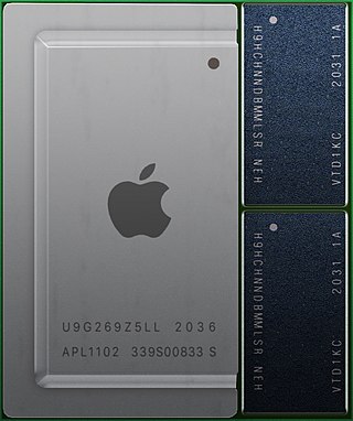
A system on a chip or system-on-chip is an integrated circuit that integrates most or all components of a computer or other electronic system. These components almost always include on-chip central processing unit (CPU), memory interfaces, input/output devices and interfaces, and secondary storage interfaces, often alongside other components such as radio modems and a graphics processing unit (GPU) – all on a single substrate or microchip. SoCs may contain digital and also analog, mixed-signal and often radio frequency signal processing functions.

<span class="mw-page-title-main">Application-specific integrated circuit</span> Integrated circuit customized for a specific task

An application-specific integrated circuit is an integrated circuit (IC) chip customized for a particular use, rather than intended for general-purpose use, such as a chip designed to run in a digital voice recorder or a high-efficiency video codec. Application-specific standard product chips are intermediate between ASICs and industry standard integrated circuits like the 7400 series or the 4000 series. ASIC chips are typically fabricated using metal–oxide–semiconductor (MOS) technology, as MOS integrated circuit chips.

<span class="mw-page-title-main">Clock signal</span> Timing of electronic circuits

In electronics and especially synchronous digital circuits, a clock signal is an electronic logic signal which oscillates between a high and a low state at a constant frequency and is used like a metronome to synchronize actions of digital circuits. In a synchronous logic circuit, the most common type of digital circuit, the clock signal is applied to all storage devices, flip-flops and latches, and causes them all to change state simultaneously, preventing race conditions.

Electronic design automation (EDA), also referred to as electronic computer-aided design (ECAD), is a category of software tools for designing electronic systems such as integrated circuits and printed circuit boards. The tools work together in a design flow that chip designers use to design and analyze entire semiconductor chips. Since a modern semiconductor chip can have billions of components, EDA tools are essential for their design; this article in particular describes EDA specifically with respect to integrated circuits (ICs).

Formal equivalence checking process is a part of electronic design automation (EDA), commonly used during the development of digital integrated circuits, to formally prove that two representations of a circuit design exhibit exactly the same behavior.

In computer engineering, logic synthesis is a process by which an abstract specification of desired circuit behavior, typically at register transfer level (RTL), is turned into a design implementation in terms of logic gates, typically by a computer program called a synthesis tool. Common examples of this process include synthesis of designs specified in hardware description languages, including VHDL and Verilog. Some synthesis tools generate bitstreams for programmable logic devices such as PALs or FPGAs, while others target the creation of ASICs. Logic synthesis is one step in circuit design in the electronic design automation, the others are place and route and verification and validation.

Asynchronous circuit is a sequential digital logic circuit that does not use a global clock circuit or signal generator to synchronize its components. Instead, the components are driven by a handshaking circuit which indicates a completion of a set of instructions. Handshaking works by simple data transfer protocols. Many synchronous circuits were developed in early 1950s as part of bigger asynchronous systems. Asynchronous circuits and theory surrounding is a part of several steps in integrated circuit design, a field of digital electronics engineering.

<span class="mw-page-title-main">Standard cell</span> Method of designing specialized integrated circuits

In semiconductor design, standard-cell methodology is a method of designing application-specific integrated circuits (ASICs) with mostly digital-logic features. Standard-cell methodology is an example of design abstraction, whereby a low-level very-large-scale integration (VLSI) layout is encapsulated into an abstract logic representation.

In computer architecture, clock gating is a popular power management technique used in many synchronous circuits for reducing dynamic power dissipation, by removing the clock signal when the circuit, or a subpart of it, is not in use or ignores clock signal. Clock gating saves power by pruning the clock tree, at the cost of adding more logic to a circuit. Pruning the clock disables portions of the circuitry so that the flip-flops in them do not switch state, as switching the state consumes power. When not being switched, the switching power consumption goes to zero, and only leakage currents are incurred.

<span class="mw-page-title-main">Integrated circuit design</span> Engineering process for electronic hardware

Integrated circuit design, semiconductor design, chip design or IC design, is a sub-field of electronics engineering, encompassing the particular logic and circuit design techniques required to design integrated circuits, or ICs. ICs consist of miniaturized electronic components built into an electrical network on a monolithic semiconductor substrate by photolithography.

Logic simulation is the use of simulation software to predict the behavior of digital circuits and hardware description languages. Simulation can be performed at varying degrees of physical abstraction, such as at the transistor level, gate level, register-transfer level (RTL), electronic system-level (ESL), or behavioral level.

Power optimization is the use of electronic design automation tools to optimize (reduce) the power consumption of a digital design, such as that of an integrated circuit, while preserving the functionality.

Design Closure is a part of the digital electronic design automation workflow by which an integrated circuit design is modified from its initial description to meet a growing list of design constraints and objectives.

Logic optimization is a process of finding an equivalent representation of the specified logic circuit under one or more specified constraints. This process is a part of a logic synthesis applied in digital electronics and integrated circuit design.

Retiming is the technique of moving the structural location of latches or registers in a digital circuit to improve its performance, area, and/or power characteristics in such a way that preserves its functional behavior at its outputs. Retiming was first described by Charles E. Leiserson and James B. Saxe in 1983.

<span class="mw-page-title-main">Physical design (electronics)</span>

In integrated circuit design, physical design is a step in the standard design cycle which follows after the circuit design. At this step, circuit representations of the components of the design are converted into geometric representations of shapes which, when manufactured in the corresponding layers of materials, will ensure the required functioning of the components. This geometric representation is called integrated circuit layout. This step is usually split into several sub-steps, which include both design and verification and validation of the layout.

High-level synthesis (HLS), sometimes referred to as C synthesis, electronic system-level (ESL) synthesis, algorithmic synthesis, or behavioral synthesis, is an automated design process that takes an abstract behavioral specification of a digital system and finds a register-transfer level structure that realizes the given behavior.

Catapult C Synthesis, a commercial electronic design automation product of Mentor Graphics, is a high-level synthesis tool, sometimes called algorithmic synthesis or ESL synthesis. Catapult C takes ANSI C/C++ and SystemC inputs and generates register transfer level (RTL) code targeted to FPGAs and ASICs.

References

  1. Frank Vahid (2010). Digital Design with RTL Design, Verilog and VHDL (2nd ed.). John Wiley and Sons. p. 247. ISBN   978-0-470-53108-2.
  2. Yosys Manual (RTLIL)
  3. "Power Estimation Techniques for Integrated Circuits "
  4. "Low-Power Architectural Design Methodologies "
  5. "Register-Transfer Level Estimation Techniques for Switching Activity and Power Consumption"
  6. "Power Macromodeling for High Level Power Estimationy"