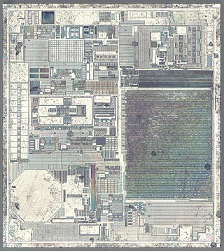
A semiconductor is a material which has an electrical conductivity value falling between that of a conductor, such as copper, and an insulator, such as glass. Its resistivity falls as its temperature rises; metals behave in the opposite way. Its conducting properties may be altered in useful ways by introducing impurities ("doping") into the crystal structure. When two differently doped regions exist in the same crystal, a semiconductor junction is created. The behavior of charge carriers, which include electrons, ions, and electron holes, at these junctions is the basis of diodes, transistors, and most modern electronics. Some examples of semiconductors are silicon, germanium, gallium arsenide, and elements near the so-called "metalloid staircase" on the periodic table. After silicon, gallium arsenide is the second-most common semiconductor and is used in laser diodes, solar cells, microwave-frequency integrated circuits, and others. Silicon is a critical element for fabricating most electronic circuits.

Electrostatic discharge (ESD) is a sudden and momentary flow of electric current between two electrically charged objects caused by contact, an electrical short or dielectric breakdown. A buildup of static electricity can be caused by tribocharging or by electrostatic induction. The ESD occurs when differently-charged objects are brought close together or when the dielectric between them breaks down, often creating a visible spark.
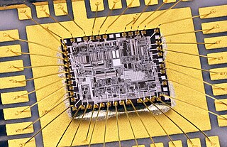
Wire bonding is the method of making interconnections between an integrated circuit (IC) or other semiconductor device and its packaging during semiconductor device fabrication. Although less common, wire bonding can be used to connect an IC to other electronics or to connect from one printed circuit board (PCB) to another. Wire bonding is generally considered the most cost-effective and flexible interconnect technology and is used to assemble the vast majority of semiconductor packages. Wire bonding can be used at frequencies above 100 GHz.

Electromigration is the transport of material caused by the gradual movement of the ions in a conductor due to the momentum transfer between conducting electrons and diffusing metal atoms. The effect is important in applications where high direct current densities are used, such as in microelectronics and related structures. As the structure size in electronics such as integrated circuits (ICs) decreases, the practical significance of this effect increases.
Nanoelectromechanical systems (NEMS) are a class of devices integrating electrical and mechanical functionality on the nanoscale. NEMS form the next logical miniaturization step from so-called microelectromechanical systems, or MEMS devices. NEMS typically integrate transistor-like nanoelectronics with mechanical actuators, pumps, or motors, and may thereby form physical, biological, and chemical sensors. The name derives from typical device dimensions in the nanometer range, leading to low mass, high mechanical resonance frequencies, potentially large quantum mechanical effects such as zero point motion, and a high surface-to-volume ratio useful for surface-based sensing mechanisms. Applications include accelerometers and sensors to detect chemical substances in the air.
Radiation hardening is the process of making electronic components and circuits resistant to damage or malfunction caused by high levels of ionizing radiation, especially for environments in outer space, around nuclear reactors and particle accelerators, or during nuclear accidents or nuclear warfare.
Reliability engineering is a sub-discipline of systems engineering that emphasizes the ability of equipment to function without failure. Reliability describes the ability of a system or component to function under stated conditions for a specified period of time. Reliability is closely related to availability, which is typically described as the ability of a component or system to function at a specified moment or interval of time.
Integrated logistic support (ILS) is a technology in the system engineering to lower a product life cycle cost and decrease demand for logistics by the maintenance system optimization to ease the product support. Although originally developed for military purposes, it is also widely used in commercial customer service organisations.
Environmental stress screening (ESS) refers to the process of exposing a newly manufactured or repaired product or component to stresses such as thermal cycling and vibration in order to force latent defects to manifest themselves by permanent or catastrophic failure during the screening process. The surviving population, upon completion of screening, can be assumed to have a higher reliability than a similar unscreened population.

All electronic devices and circuitry generate excess heat and thus require thermal management to improve reliability and prevent premature failure. The amount of heat output is equal to the power input, if there are no other energy interactions. There are several techniques for cooling including various styles of heat sinks, thermoelectric coolers, forced air systems and fans, heat pipes, and others. In cases of extreme low environmental temperatures, it may actually be necessary to heat the electronic components to achieve satisfactory operation.
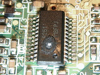
Electronic packaging is the design and production of enclosures for electronic devices ranging from individual semiconductor devices up to complete systems such as a mainframe computer. Packaging of an electronic system must consider protection from mechanical damage, cooling, radio frequency noise emission and electrostatic discharge. Product safety standards may dictate particular features of a consumer product, for example, external case temperature or grounding of exposed metal parts. Prototypes and industrial equipment made in small quantities may use standardized commercially available enclosures such as card cages or prefabricated boxes. Mass-market consumer devices may have highly specialized packaging to increase consumer appeal. Electronic packaging is a major discipline within the field of mechanical engineering.
Worst-case circuit analysis is a cost-effective means of screening a design to ensure with a high degree of confidence that potential defects and deficiencies are identified and eliminated prior to and during test, production, and delivery.
The MIL-STD-883 standard establishes uniform methods, controls, and procedures for testing microelectronic devices suitable for use within military and aerospace electronic systems including basic environmental tests to determine resistance to deleterious effects of natural elements and conditions surrounding military and space operations; mechanical and electrical tests; workmanship and training procedures; and such other controls and constraints as have been deemed necessary to ensure a uniform level of quality and reliability suitable to the intended applications of those devices. For this standard, the term "devices" includes monolithic, multichip, film and hybrid microcircuits, microcircuit arrays, and the elements from which the circuits and arrays are formed. This standard is intended to apply only to microelectronic devices.

A tantalum electrolytic capacitor is an electrolytic capacitor, a passive component of electronic circuits. It consists of a pellet of porous tantalum metal as an anode, covered by an insulating oxide layer that forms the dielectric, surrounded by liquid or solid electrolyte as a cathode. Because of its very thin and relatively high permittivity dielectric layer, the tantalum capacitor distinguishes itself from other conventional and electrolytic capacitors in having high capacitance per volume and lower weight.
An operating temperature is the allowable temperature range of the local ambient environment at which an electrical or mechanical device operates. The device will operate effectively within a specified temperature range which varies based on the device function and application context, and ranges from the minimum operating temperature to the maximum operating temperature. Outside this range of safe operating temperatures the device may fail.
Electronic components have a wide range of failure modes. These can be classified in various ways, such as by time or cause. Failures can be caused by excess temperature, excess current or voltage, ionizing radiation, mechanical shock, stress or impact, and many other causes. In semiconductor devices, problems in the device package may cause failures due to contamination, mechanical stress of the device, or open or short circuits.
Physics of failure is a technique under the practice of reliability design that leverages the knowledge and understanding of the processes and mechanisms that induce failure to predict reliability and improve product performance.
Sherlock Automated Design Analysis is a software tool developed by DfR Solutions for analyzing, grading, and certifying the expected reliability of products at the circuit card assembly level. Based on the science of Physics of Failure, Sherlock predicts failure mechanism-specific failure rates over time using a combination of finite element method and material properties to capture stress values and first order analytical equations to evaluate damage evolution. The software is designed for use by design and reliability engineers and managers in the electronics industry. DfR Solutions is based in Beltsville, Maryland, USA, and was acquired by ANSYS, Inc. in May 2019.
Robustness validation is a skills strategy with which the Robustness of a product to the loading conditions of a real application is proven and targeted statements about risks and reliability can be made. This strategy is particularly for use in the automotive industry however could be applied to any industry where high levels of reliability are required