| Group | Elem. | Material | Formula | Band gap (eV) | Gap type | Description |
|---|
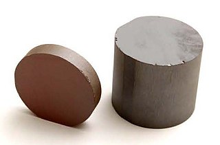
| IV | 1 | Silicon | Si | 1.12 [5] [6] | indirect | Used in conventional crystalline silicon (c-Si) solar cells, and in its amorphous form as amorphous silicon (a-Si) in thin-film solar cells. Most common semiconductor material in photovoltaics; dominates worldwide PV market; easy to fabricate; good electrical and mechanical properties. Forms high quality thermal oxide for insulation purposes. Most common material used in the fabrication of Integrated Circuits. |
| IV | 1 | Germanium | Ge | 0.67 [5] [6] | indirect | Used in early radar detection diodes and first transistors; requires lower purity than silicon. A substrate for high-efficiency multijunction photovoltaic cells. Very similar lattice constant to gallium arsenide. High-purity crystals used for gamma spectroscopy. May grow whiskers, which impair reliability of some devices. |
| IV | 1 | Diamond | C | 5.47 [5] [6] | indirect | Excellent thermal conductivity. Superior mechanical and optical properties. High carrier mobilities [7] and high electric breakdown field [8] at room temperature as excellent electronics characteristics. Extremely high nanomechanical resonator quality factor. [9] |
| IV | 1 | Gray tin, α-Sn | Sn | 0 [10] [11] | semimetal | Low temperature allotrope (diamond cubic lattice). |
| IV | 2 | Silicon carbide, 3C-SiC | SiC | 2.3 [5] | indirect | used for early yellow LEDs |
| IV | 2 | Silicon carbide, 4H-SiC | SiC | 3.3 [5] | indirect | Used for high-voltage and high-temperature applications |
| IV | 2 | Silicon carbide, 6H-SiC | SiC | 3.0 [5] | indirect | used for early blue LEDs |
| VI | 1 | Sulfur, α-S | S8 | 2.6 [12] | | |
| VI | 1 | Gray (trigonal) selenium | Se | 1.83 - 2.0 [13] [14] | indirect | Used in selenium rectifiers and solar cells. [15] Band gap depends on fabrication conditions. |
| VI | 1 | Red selenium | Se | 2.05 | indirect | [16] |
| VI | 1 | Tellurium | Te | 0.33 [17] | | |
| III-V | 2 | Boron nitride, cubic | BN | 6.36 [18] | indirect | potentially useful for ultraviolet LEDs |
| III-V | 2 | Boron nitride, hexagonal | BN | 5.96 [18] | quasi-direct | potentially useful for ultraviolet LEDs |
| III-V | 2 | Boron nitride nanotube | BN | 5.5 [19] | | |
| III-V | 2 | Boron phosphide | BP | 2.1 [20] | indirect | |
| III-V | 2 | Boron arsenide | BAs | 1.82 | direct | Ultrahigh thermal conductivity for thermal management; Resistant to radiation damage, possible applications in betavoltaics. |
| III-V | 2 | Boron arsenide | B12As2 | 3.47 | indirect | Resistant to radiation damage, possible applications in betavoltaics. |
| III-V | 2 | Aluminium nitride | AlN | 6.28 [5] | direct | Piezoelectric. Not used on its own as a semiconductor; AlN-close GaAlN possibly usable for ultraviolet LEDs. Inefficient emission at 210 nm was achieved on AlN. |
| III-V | 2 | Aluminium phosphide | AlP | 2.45 [6] | indirect | |
| III-V | 2 | Aluminium arsenide | AlAs | 2.16 [6] | indirect | |
| III-V | 2 | Aluminium antimonide | AlSb | 1.6/2.2 [6] | indirect/direct | |
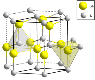
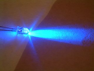
| III-V | 2 | Gallium nitride | GaN | 3.44 [5] [6] | direct | problematic to be doped to p-type, p-doping with Mg and annealing allowed first high-efficiency blue LEDs [3] and blue lasers. Very sensitive to ESD. Insensitive to ionizing radiation. GaN transistors can operate at higher voltages and higher temperatures than GaAs, used in microwave power amplifiers. When doped with e.g. manganese, becomes a magnetic semiconductor. |
| III-V | 2 | Gallium phosphide | GaP | 2.26 [5] [6] | indirect | Used in early low to medium brightness cheap red/orange/green LEDs. Used standalone or with GaAsP. Transparent for yellow and red light, used as substrate for GaAsP red/yellow LEDs. Doped with S or Te for n-type, with Zn for p-type. Pure GaP emits green, nitrogen-doped GaP emits yellow-green, ZnO-doped GaP emits red. |
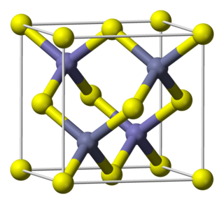
| III-V | 2 | Gallium arsenide | GaAs | 1.42 [5] [6] | direct | second most common in use after silicon, commonly used as substrate for other III-V semiconductors, e.g. InGaAs and GaInNAs. Brittle. Lower hole mobility than Si, P-type CMOS transistors unfeasible. High impurity density, difficult to fabricate small structures. Used for near-IR LEDs, fast electronics, and high-efficiency solar cells. Very similar lattice constant to germanium, can be grown on germanium substrates. |
| III-V | 2 | Gallium antimonide | GaSb | 0.73 [5] [6] | direct | Used for infrared detectors and LEDs and thermophotovoltaics. Doped n with Te, p with Zn. |
| III-V | 2 | Indium nitride | InN | 0.7 [5] | direct | Possible use in solar cells, but p-type doping difficult. Used frequently as alloys. |
| III-V | 2 | Indium phosphide | InP | 1.35 [5] | direct | Commonly used as substrate for epitaxial InGaAs. Superior electron velocity, used in high-power and high-frequency applications. Used in optoelectronics. |
| III-V | 2 | Indium arsenide | InAs | 0.36 [5] | direct | Used for infrared detectors for 1–3.8 μm, cooled or uncooled. High electron mobility. InAs dots in InGaAs matrix can serve as quantum dots. Quantum dots may be formed from a monolayer of InAs on InP or GaAs. Strong photo-Dember emitter, used as a terahertz radiation source. |
| III-V | 2 | Indium antimonide | InSb | 0.17 [5] | direct | Used in infrared detectors and thermal imaging sensors, high quantum efficiency, low stability, require cooling, used in military long-range thermal imager systems. AlInSb-InSb-AlInSb structure used as quantum well. Very high electron mobility, electron velocity and ballistic length. Transistors can operate below 0.5V and above 200 GHz. Terahertz frequencies maybe achievable. |
| II-VI | 2 | Cadmium selenide | CdSe | 1.74 [6] | direct | Nanoparticles used as quantum dots. Intrinsic n-type, difficult to dope p-type, but can be p-type doped with nitrogen. Possible use in optoelectronics. Tested for high-efficiency solar cells. |
| II-VI | 2 | Cadmium sulfide | CdS | 2.42 [6] | direct | Used in photoresistors and solar cells; CdS/Cu2S was the first efficient solar cell. Used in solar cells with CdTe. Common as quantum dots. Crystals can act as solid-state lasers. Electroluminescent. When doped, can act as a phosphor. |
| II-VI | 2 | Cadmium telluride | CdTe | 1.49 [6] | direct | Used in solar cells with CdS. Used in thin film solar cells and other cadmium telluride photovoltaics; less efficient than crystalline silicon but cheaper. High electro-optic effect, used in electro-optic modulators. Fluorescent at 790 nm. Nanoparticles usable as quantum dots. |
| II-VI, oxide | 2 | Zinc oxide | ZnO | 3.37 [6] | direct | Photocatalytic. Band gap is tunable from 3 to 4 eV by alloying with magnesium oxide and cadmium oxide. Intrinsic n-type, p-type doping is difficult. Heavy aluminium, indium, or gallium doping yields transparent conductive coatings; ZnO:Al is used as window coatings transparent in visible and reflective in infrared region and as conductive films in LCD displays and solar panels as a replacement of indium tin oxide. Resistant to radiation damage. Possible use in LEDs and laser diodes. Possible use in random lasers. |
| II-VI | 2 | Zinc selenide | ZnSe | 2.7 [6] | direct | Used for blue lasers and LEDs. Easy to n-type doping, p-type doping is difficult but can be done with e.g. nitrogen. Common optical material in infrared optics. |
| II-VI | 2 | Zinc sulfide | ZnS | 3.54/3.91 [6] | direct | Band gap 3.54 eV (cubic), 3.91 (hexagonal). Can be doped both n-type and p-type. Common scintillator/phosphor when suitably doped. |
| II-VI | 2 | Zinc telluride | ZnTe | 2.3 [6] | direct | Can be grown on AlSb, GaSb, InAs, and PbSe. Used in solar cells, components of microwave generators, blue LEDs and lasers. Used in electrooptics. Together with lithium niobate used to generate terahertz radiation. |
| I-VII | 2 | Cuprous chloride | CuCl | 3.4 [21] | direct | |
| I-VI | 2 | Copper sulfide | Cu2S | 1.2 [20] | indirect | p-type, Cu2S/CdS was the first efficient thin film solar cell |
| IV-VI | 2 | Lead selenide | PbSe | 0.26 [17] | direct | Used in infrared detectors for thermal imaging. Nanocrystals usable as quantum dots. Good high temperature thermoelectric material. |
| IV-VI | 2 | Lead(II) sulfide | PbS | 0.37 [22] | | Mineral galena, first semiconductor in practical use, used in cat's whisker detectors; the detectors are slow due to high dielectric constant of PbS. Oldest material used in infrared detectors. At room temperature can detect SWIR, longer wavelengths require cooling. |
| IV-VI | 2 | Lead telluride | PbTe | 0.32 [5] | | Low thermal conductivity, good thermoelectric material at elevated temperature for thermoelectric generators. |
| IV-VI | 2 | Tin(II) sulfide | SnS | 1.3/1.0 [23] | direct/indirect | Tin sulfide (SnS) is a semiconductor with direct optical band gap of 1.3 eV and absorption coefficient above 104 cm−1 for photon energies above 1.3 eV. It is a p-type semiconductor whose electrical properties can be tailored by doping and structural modification and has emerged as one of the simple, non-toxic and affordable material for thin films solar cells since a decade. |
| IV-VI | 2 | Tin(IV) sulfide | SnS2 | 2.2 [24] | | SnS2 is widely used in gas sensing applications. |
| IV-VI | 2 | Tin telluride | SnTe | 0.18 | | Complex band structure. |
| IV-VI | 3 | Lead tin telluride | Pb1−xSnxTe | 0-0.29 | | Used in infrared detectors and for thermal imaging |
| V-VI, layered | 2 | Bismuth telluride | Bi2Te3 | 0.13 [5] | | Efficient thermoelectric material near room temperature when alloyed with selenium or antimony. Narrow-gap layered semiconductor. High electrical conductivity, low thermal conductivity. Topological insulator. |
| II-V | 2 | Cadmium phosphide | Cd3P2 | 0.5 [25] | | |
| II-V | 2 | Cadmium arsenide | Cd3As2 | 0 | | N-type intrinsic semiconductor. Very high electron mobility. Used in infrared detectors, photodetectors, dynamic thin-film pressure sensors, and magnetoresistors. Recent measurements suggest that 3D Cd3As2 is actually a zero band-gap Dirac semimetal in which electrons behave relativistically as in graphene. [26] |
| II-V | 2 | Zinc phosphide | Zn3P2 | 1.5 [27] | direct | Usually p-type. |
| II-V | 2 | Zinc diphosphide | ZnP2 | 2.1 [28] | | |
| II-V | 2 | Zinc arsenide | Zn3As2 | 1.0 [29] | | The lowest direct and indirect bandgaps are within 30 meV or each other. [29] |
| II-V | 2 | Zinc antimonide | Zn3Sb2 | | | Used in infrared detectors and thermal imagers, transistors, and magnetoresistors. |
| Oxide | 2 | Titanium dioxide, anatase | TiO2 | 3.20 [30] | indirect | photocatalytic, n-type |
| Oxide | 2 | Titanium dioxide, rutile | TiO2 | 3.0 [30] | direct | photocatalytic, n-type |
| Oxide | 2 | Titanium dioxide, brookite | TiO2 | 3.26 [30] | | [31] |
| Oxide | 2 | Copper(I) oxide | Cu2O | 2.17 [32] | | One of the most studied semiconductors. Many applications and effects first demonstrated with it. Formerly used in rectifier diodes, before silicon. |
| Oxide | 2 | Copper(II) oxide | CuO | 1.2 | | N-type semiconductor. [33] |
| Oxide | 2 | Uranium dioxide | UO2 | 1.3 | | High Seebeck coefficient, resistant to high temperatures, promising thermoelectric and thermophotovoltaic applications. Formerly used in URDOX resistors, conducting at high temperature. Resistant to radiation damage. |
| Oxide | 2 | Tin dioxide | SnO2 | 3.7 | | Oxygen-deficient n-type semiconductor. Used in gas sensors. |
| Oxide | 3 | Barium titanate | BaTiO3 | 3 | | Ferroelectric, piezoelectric. Used in some uncooled thermal imagers. Used in nonlinear optics. |
| Oxide | 3 | Strontium titanate | SrTiO3 | 3.3 | | Ferroelectric, piezoelectric. Used in varistors. Conductive when niobium-doped. |
| Oxide | 3 | Lithium niobate | LiNbO3 | 4 | | Ferroelectric, piezoelectric, shows Pockels effect. Wide uses in electrooptics and photonics. |
| V-VI | 2 | monoclinic Vanadium(IV) oxide | VO2 | 0.7 [34] | optical | stable below 67 °C |
| Layered | 2 | Lead(II) iodide | PbI2 | 2.4 [35] | | PbI2 is a layered direct bandgap semiconductor with bandgap of 2.4 eV in its bulk form, whereas its 2D monolayer has an indirect bandgap of ~2.5 eV, with possibilities to tune the bandgap between 1–3 eV |
| Layered | 2 | Molybdenum disulfide | MoS2 | 1.23 eV (2H) [36] | indirect | |
| Layered | 2 | Gallium selenide | GaSe | 2.1 | indirect | Photoconductor. Uses in nonlinear optics. Used as 2D-material. Air sensitive. [37] [38] [39] |
| Layered | 2 | Indium selenide | InSe | 1.26-2.35 eV [39] | direct (indirect in 2D) | Air sensitive. High electrical mobility in few- and mono-layer form. [37] [38] [39] |
| Layered | 2 | Tin sulfide | SnS | >1.5 eV | direct | |
| Layered | 2 | Bismuth sulfide | Bi2S3 | 1.3 [5] | | |
| Magnetic, diluted (DMS) [40] | 3 | Gallium manganese arsenide | GaMnAs | | | |
| Magnetic, diluted (DMS) | 3 | Lead manganese telluride | PbMnTe | | | |
| Magnetic | 4 | Lanthanum calcium manganate | La0.7Ca0.3MnO3 | | | colossal magnetoresistance |
| Magnetic | 2 | Iron(II) oxide | FeO | 2.2 [41] | | antiferromagnetic Band gap for iron oxide nanoparticles was found to be 2.2 eV and on doping the band gap found to be increased up to 2.5 eV |
| Magnetic | 2 | Nickel(II) oxide | NiO | 3.6–4.0 | direct [42] [43] | antiferromagnetic |
| Magnetic | 2 | Europium(II) oxide | EuO | | | ferromagnetic |
| Magnetic | 2 | Europium(II) sulfide | EuS | | | ferromagnetic |
| Magnetic | 2 | Chromium(III) bromide | CrBr3 | | | |
| other | 3 | Copper indium selenide, CIS | CuInSe2 | 1 | direct | |
| other | 3 | Silver gallium sulfide | AgGaS2 | | | nonlinear optical properties |
| other | 3 | Zinc silicon phosphide | ZnSiP2 | 2.0 [20] | | |
| other | 2 | Arsenic trisulfide Orpiment | As2S3 | 2.7 [44] | direct | semiconductive in both crystalline and glassy state |
| other | 2 | Arsenic sulfide Realgar | As4S4 | | | semiconductive in both crystalline and glassy state |
| other | 2 | Platinum silicide | PtSi | | | Used in infrared detectors for 1–5 μm. Used in infrared astronomy. High stability, low drift, used for measurements. Low quantum efficiency. |
| other | 2 | Bismuth(III) iodide | BiI3 | | | |
| other | 2 | Mercury(II) iodide | HgI2 | | | Used in some gamma-ray and x-ray detectors and imaging systems operating at room temperature. |
| other | 2 | Thallium(I) bromide | TlBr | 2.68 [45] | | Used in some gamma-ray and x-ray detectors and imaging systems operating at room temperature. Used as a real-time x-ray image sensor. |
| other | 2 | Silver sulfide | Ag2S | 0.9 [46] | | |
| other | 2 | Iron disulfide | FeS2 | 0.95 [47] | | Mineral pyrite. Used in later cat's whisker detectors, investigated for solar cells. |
| other | 4 | Copper zinc tin sulfide, CZTS | Cu2ZnSnS4 | 1.49 | direct | Cu2ZnSnS4 is derived from CIGS, replacing the Indium/Gallium with earth abundant Zinc/Tin. |
| other | 4 | Copper zinc antimony sulfide, CZAS | Cu1.18Zn0.40Sb1.90S7.2 | 2.2 [48] | direct | Copper zinc antimony sulfide is derived from copper antimony sulfide (CAS), a famatinite class of compound. |
| other | 3 | Copper tin sulfide, CTS | Cu2SnS3 | 0.91 [20] | direct | Cu2SnS3 is p-type semiconductor and it can be used in thin film solar cell application. |