
Aluminium gallium arsenide (AlxGa1−xAs) is a semiconductor material with very nearly the same lattice constant as GaAs, but a larger bandgap. The x in the formula above is a number between 0 and 1 - this indicates an arbitrary alloy between GaAs and AlAs.

A laser diode is a semiconductor device similar to a light-emitting diode in which a diode pumped directly with electrical current can create lasing conditions at the diode's junction.

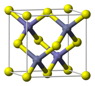
Gallium arsenide (GaAs) is a III-V direct band gap semiconductor with a zinc blende crystal structure.

Epitaxy refers to a type of crystal growth or material deposition in which new crystalline layers are formed with one or more well-defined orientations with respect to the crystalline seed layer. The deposited crystalline film is called an epitaxial film or epitaxial layer. The relative orientation(s) of the epitaxial layer to the seed layer is defined in terms of the orientation of the crystal lattice of each material. For most epitaxial growths, the new layer is usually crystalline and each crystallographic domain of the overlayer must have a well-defined orientation relative to the substrate crystal structure. Epitaxy can involve single-crystal structures, although grain-to-grain epitaxy has been observed in granular films. For most technological applications, single domain epitaxy, which is the growth of an overlayer crystal with one well-defined orientation with respect to the substrate crystal, is preferred. Epitaxy can also play an important role while growing superlattice structures.
The heterojunction bipolar transistor (HBT) is a type of bipolar junction transistor (BJT) which uses differing semiconductor materials for the emitter and base regions, creating a heterojunction. The HBT improves on the BJT in that it can handle signals of very high frequencies, up to several hundred GHz. It is commonly used in modern ultrafast circuits, mostly radio frequency (RF) systems, and in applications requiring a high power efficiency, such as RF power amplifiers in cellular phones. The idea of employing a heterojunction is as old as the conventional BJT, dating back to a patent from 1951. Detailed theory of heterojunction bipolar transistor was developed by Herbert Kroemer in 1957.
Indium antimonide (InSb) is a crystalline compound made from the elements indium (In) and antimony (Sb). It is a narrow-gap semiconductor material from the III-V group used in infrared detectors, including thermal imaging cameras, FLIR systems, infrared homing missile guidance systems, and in infrared astronomy. Indium antimonide detectors are sensitive to infrared wavelengths between 1 and 5 μm.
Indium gallium phosphide (InGaP), also called gallium indium phosphide (GaInP), is a semiconductor composed of indium, gallium and phosphorus. It is used in high-power and high-frequency electronics because of its superior electron velocity with respect to the more common semiconductors silicon and gallium arsenide.
Indium gallium arsenide (InGaAs) is a ternary alloy of indium arsenide (InAs) and gallium arsenide (GaAs). Indium and gallium are group III elements of the periodic table while arsenic is a group V element. Alloys made of these chemical groups are referred to as "III-V" compounds. InGaAs has properties intermediate between those of GaAs and InAs. InGaAs is a room-temperature semiconductor with applications in electronics and photonics.

Hg1−xCdxTe or mercury cadmium telluride is a chemical compound of cadmium telluride (CdTe) and mercury telluride (HgTe) with a tunable bandgap spanning the shortwave infrared to the very long wave infrared regions. The amount of cadmium (Cd) in the alloy can be chosen so as to tune the optical absorption of the material to the desired infrared wavelength. CdTe is a semiconductor with a bandgap of approximately 1.5 electronvolts (eV) at room temperature. HgTe is a semimetal, which means that its bandgap energy is zero. Mixing these two substances allows one to obtain any bandgap between 0 and 1.5 eV.
Indium gallium nitride is a semiconductor material made of a mix of gallium nitride (GaN) and indium nitride (InN). It is a ternary group III/group V direct bandgap semiconductor. Its bandgap can be tuned by varying the amount of indium in the alloy. InxGa1−xN has a direct bandgap span from the infrared for InN to the ultraviolet of GaN. The ratio of In/Ga is usually between 0.02/0.98 and 0.3/0.7.
Aluminium gallium indium phosphide is a semiconductor material that provides a platform for the development of novel multi-junction photovoltaics and optoelectronic devices, as it spans a direct bandgap from deep ultraviolet to infrared.

Aluminium antimonide (AlSb) is a semiconductor of the group III-V family containing aluminium and antimony. The lattice constant is 0.61 nm. The indirect bandgap is approximately 1.6 eV at 300 K, whereas the direct band gap is 2.22 eV.
Gallium antimonide (GaSb) is a semiconducting compound of gallium and antimony of the III-V family. It has a room temperature lattice constant of about 0.610 nm. It has a room temperature direct bandgap of approximately 0.73 eV.
Aluminium indium arsenide, also indium aluminium arsenide or AlInAs (AlxIn1−xAs), is a semiconductor material with very nearly the same lattice constant as GaInAs, but a larger bandgap. The x in the formula above is a number between 0 and 1 - this indicates an arbitrary alloy between InAs and AlAs.
A quantum well laser is a laser diode in which the active region of the device is so narrow that quantum confinement occurs. Laser diodes are formed in compound semiconductor materials that are able to emit light efficiently. The wavelength of the light emitted by a quantum well laser is determined by the width of the active region rather than just the bandgap of the materials from which it is constructed. This means that much shorter wavelengths can be obtained from quantum well lasers than from conventional laser diodes using a particular semiconductor material. The efficiency of a quantum well laser is also greater than a conventional laser diode due to the stepwise form of its density of states function.
Aluminium indium antimonide, also known as indium aluminium antimonide or AlInSb (AlxIn1-xSb), is a ternary III-V semiconductor compound. The alloy can contain any ratio between aluminium and indium; that is, x in the formula can continuously take on any value between 0 and 1. AlInSb refers generally to any composition of the alloy.
Aluminium gallium antimonide, also known as gallium aluminium antimonide or AlGaSb (AlxGa1-xSb), is a ternary III-V semiconductor compound. The alloy can contain any ratio between aluminium and gallium; that is, x in the formula can continuously take on any value between 0 and 1. AlGaSb refers generally to any composition of the alloy.
Indium arsenide antimonide, also known as indium antimonide arsenide or InAsSb (InAs1-xSbx), is a ternary III-V semiconductor compound. It can be considered as an alloy between indium arsenide (InAs) and indium antimonide (InSb). x indicates the fractions of arsenic and antimony in the alloy according to the aforementioned formula; it can take on any value between 0 and 1. InAsSb refers generally to any composition of the alloy.
Gallium indium antimonide, also known as indium gallium antimonide, GaInSb, or InGaSb (GaxIn1-xSb), is a ternary III-V semiconductor compound. The alloy can contain any ratio between gallium and indium; that is, x in the formula can continuously take on any value between 0 and 1. GaInSb refers generally to any composition of the alloy.
