Transmeta Crusoe

Last updated
A Transmeta Crusoe KL Transmeta Crusoe 5800.jpg
A Transmeta Crusoe

The Transmeta Crusoe is a family of x86-compatible microprocessors developed by Transmeta and introduced in 2000.

Contents

Instead of the instruction set architecture being implemented in hardware, or translated by specialized hardware, the Crusoe runs a software abstraction layer, or a virtual machine, known as the Code Morphing Software (CMS). The CMS translates machine code instructions received from programs into native instructions for the microprocessor. In this way, the Crusoe can emulate other instruction set architectures (ISAs). This is used to allow the microprocessors to emulate the Intel x86 instruction set.

Photo of CPUID for Transmeta Crusoe TM5800 800 MHz on Fujitsu P2040 Photo of CPUID for Transmeta Crusoe TM5800 800Mhz on Fujitsu P2040.jpg
Photo of CPUID for Transmeta Crusoe TM5800 800 MHz on Fujitsu P2040

Design

A Transmeta CPU from a Fujitsu Lifebook P series laptop Transmeta TM5600.jpg
A Transmeta CPU from a Fujitsu Lifebook P series laptop

The Crusoe is notable for its method of achieving x86 compatibility. Instead of the instruction set architecture being implemented in hardware, or translated by specialized hardware, the Crusoe runs a software abstraction layer, or a virtual machine, known as the Code Morphing Software (CMS). The CMS translates machine code instructions received from programs into native instructions for the microprocessor. In this way, the Crusoe can emulate other instruction set architectures (ISAs). This is used to allow the microprocessors to emulate the Intel x86 instruction set. In theory, it is possible for the CMS to be modified to emulate other ISAs. Transmeta demonstrated Crusoe executing Java bytecode by translating the bytecodes into instructions in its native instruction set. The addition of an abstraction layer between the x86 instruction stream and the hardware means that the hardware architecture can change without breaking compatibility, just by modifying the CMS. For example, Transmeta Efficeon — a second-generation Transmeta design — has a 256-bit-wide VLIW core versus the 128-bit core of the Crusoe. Efficeon also supports SSE instructions.

The Crusoe is a VLIW microprocessor that executes bundles of instructions, termed molecules by Transmeta. Each molecule contains multiple instructions, termed atoms. The Code Morphing Software translates x86 instructions into native instructions. The native instructions are 32 bits long. Instructions that meet a set of conditions can be executed simultaneously and are combined to form a 64- or 128-bit molecule containing two or four atoms, respectively. In the event that there are not enough instructions to fill a molecule, the software inserts NOPs as padding to fill out empty slots. This is required in all VLIW architectures and is criticised for being inefficient, which is why there are molecules of two separate lengths.

The Crusoe performs in software some of the functionality traditionally implemented in hardware (e.g. instruction re-ordering), resulting in simpler hardware with fewer transistors. The relative simplicity of the hardware means that Crusoe consumes less power (and therefore generates less heat) than other x86-compatible microprocessors running at the same frequency. A 700 MHz Crusoe ran x86 programs at the speed of a 500 MHz Pentium III x86 processor, [1] although the Crusoe processor was smaller and cheaper than the corresponding Intel processor. [1]

The Crusoe was initially available in two forms: the TM3120 (later called TM3200) for embedded applications and the TM5400 for low-power personal computing. [2] Both were based on the same architecture but differed in clock frequency and peripheral support. The TM3120/TM3200 were manufactured in speeds of 333(TM3120 only) 366 and, 400 MHz using a 220 nm process. [3] [4] [5] It has a 96k L1 cache (64 KB instruction and 32 KB data) and no L2 cache. The TM3120/TM3200 has an integrated SDRAM memory controller and a PCI interface. It measures 77 mm² and uses a 1.5 V power supply, dissipating less than 1.5 W of power (typically). [3] [4] [5] The TM5400 differs from the TM3120/TM3200 with the inclusion of a 128K of L1 Cache(with the addition of 32 KB data cache) as well as the addition of DDR memory support, 256 KB unified L2 cache and LongRun power reduction technology manufactured using a smaller 180 nm process. [3] [6] It measures 73 mm² and uses a 1.10 V (f = 25%) and 1.6 V (f = 100%) power supply, dissipating 0.5–1.5 W typically and a maximum of 6 W. [3] [6] Later the TM5600 was introduced as a higher end offering to the TM5400 with double the L2 cache (512 KB vs 256 KB). [6] [7] [8] Both the TM5400 and TM5600 operated at clock frequencies of 500–700 MHz. [9]

The TM5500/TM5800 are die shrunk versions of the TM5400/5600 Built on a TSMC 130 nm process at clock frequencies of 667-1000 MHz. [10] [11] [12] Embedded versions rated for 10 years of continuous use were marketed as Crusoe SE (for Special Embedded) TM55E/TM58E respectively at clock frequencies of 667-993 MHz. [13]

The TM5700/TM5900 removes SDRAM support for its integrated memory controller and now comes in a 54% smaller 399 pin FC-OBGA package rather than the ceramic 479 BGA package used previously. [9] [12] [14] Clock speed remains the same between 667 and 1000 MHz. [15]

Production

Transmeta was a fabless semiconductor company, without the facilities to fabricate their designs. Instead, both processors were fabricated by IBM Microelectronics, the semiconductor business of International Business Machines (IBM). IBM fabricated the Crusoe in a 0.18 µm CMOS process with five levels of copper interconnect.

Software limitations

The Crusoe processor supports MMX but not SSE. [16] As of 2022, most browsers on Windows and Linux, and some other programs, need SSE or SSE2 support; [17] therefore, that software will no longer run on the Crusoe platform. For example, Firefox dropped support for systems without SSE2 in 2017, [18] although K-Meleon could run without SSE on Windows XP. The Efficeon processor added support for SSE and SSE2. [19]

Products

Related Research Articles

i386 32-bit microprocessor by Intel

The Intel 386, originally released as 80386 and later renamed i386, is a 32-bit microprocessor designed by Intel. The first pre-production samples of the 386 were released to select developers in 1985, while mass production commenced in 1986. The processor was a significant evolution in the x86 architecture, extending a long line of processors that stretched back to the Intel 8008. The 386 was the central processing unit (CPU) of many workstations and high-end personal computers of the time. The 386 began to fall out of public use starting with the release of the i486 processor in 1989, while in embedded systems the 386 remained in widespread use until Intel finally discontinued it in 2007.

<span class="mw-page-title-main">Itanium</span> Family of 64-bit Intel microprocessors

Itanium is a discontinued family of 64-bit Intel microprocessors that implement the Intel Itanium architecture. The Itanium architecture originated at Hewlett-Packard (HP), and was later jointly developed by HP and Intel. Launched in June 2001, Intel initially marketed the processors for enterprise servers and high-performance computing systems. In the concept phase, engineers said "we could run circles around PowerPC...we could kill the x86." Early predictions were that IA-64 would expand to the lower-end servers, supplanting Xeon, and eventually penetrate into the personal computers, eventually to supplant reduced instruction set computing (RISC) and complex instruction set computing (CISC) architectures for all general-purpose applications.

Very long instruction word (VLIW) refers to instruction set architectures that are designed to exploit instruction-level parallelism (ILP). A VLIW processor allows programs to explicitly specify instructions to execute in parallel, whereas conventional central processing units (CPUs) mostly allow programs to specify instructions to execute in sequence only. VLIW is intended to allow higher performance without the complexity inherent in some other designs.

In computing, Streaming SIMD Extensions (SSE) is a single instruction, multiple data (SIMD) instruction set extension to the x86 architecture, designed by Intel and introduced in 1999 in their Pentium III series of central processing units (CPUs) shortly after the appearance of Advanced Micro Devices (AMD's) 3DNow!. SSE contains 70 new instructions, most of which work on single precision floating-point data. SIMD instructions can greatly increase performance when exactly the same operations are to be performed on multiple data objects. Typical applications are digital signal processing and graphics processing.

<span class="mw-page-title-main">Duron</span> Series of CPUs by AMD

Duron is a line of budget x86-compatible microprocessors manufactured by AMD and released on June 19, 2000. Duron was intended to be a lower-cost offering to complement AMD's then mainstream performance Athlon processor line, and it also competed with rival chipmaker Intel's Pentium III and Celeron processor offerings. The Duron brand name was retired in 2004, succeeded by the AMD's Sempron line of processors as their budget offering.

<span class="mw-page-title-main">Pentium II</span> Intel microprocessor

The Pentium II brand refers to Intel's sixth-generation microarchitecture ("P6") and x86-compatible microprocessors introduced on May 7, 1997. Containing 7.5 million transistors, the Pentium II featured an improved version of the first P6-generation core of the Pentium Pro, which contained 5.5 million transistors. However, its L2 cache subsystem was a downgrade when compared to the Pentium Pros. It is a single-core microprocessor.

<span class="mw-page-title-main">Pentium III</span> Line of desktop and mobile microprocessors produced by Intel

The Pentium III brand refers to Intel's 32-bit x86 desktop and mobile CPUs based on the sixth-generation P6 microarchitecture introduced on February 28, 1999. The brand's initial processors were very similar to the earlier Pentium II-branded processors. The most notable differences were the addition of the Streaming SIMD Extensions (SSE) instruction set, and the introduction of a controversial serial number embedded in the chip during manufacturing. The Pentium III is also a single-core processor.

Transmeta Corporation was an American fabless semiconductor company based in Santa Clara, California. It developed low power x86 compatible microprocessors based on a VLIW core and a software layer called Code Morphing Software.

<span class="mw-page-title-main">Athlon 64</span> Series of CPUs by AMD

The Athlon 64 is a ninth-generation, AMD64-architecture microprocessor produced by Advanced Micro Devices (AMD), released on September 23, 2003. It is the third processor to bear the name Athlon, and the immediate successor to the Athlon XP. The Athlon 64 was the second processor to implement the AMD64 architecture and the first 64-bit processor targeted at the average consumer. Variants of the Athlon 64 have been produced for Socket 754, Socket 939, Socket 940, and Socket AM2. It was AMD's primary consumer CPU, and primarily competed with Intel's Pentium 4, especially the Prescott and Cedar Mill core revisions.

In computing, binary translation is a form of binary recompilation where sequences of instructions are translated from a source instruction set to the target instruction set. In some cases such as instruction set simulation, the target instruction set may be the same as the source instruction set, providing testing and debugging features such as instruction trace, conditional breakpoints and hot spot detection.

<span class="mw-page-title-main">AMD K6-III</span> Microprocessor series by AMD

The K6-III was an x86 microprocessor line manufactured by AMD that launched on February 22, 1999. The launch consisted of both 400 and 450 MHz models and was based on the preceding K6-2 architecture. Its improved 256 KB on-chip L2 cache gave it significant improvements in system performance over its predecessor the K6-2. The K6-III was the last processor officially released for desktop Socket 7 systems, however later mobile K6-III+ and K6-2+ processors could be run unofficially in certain socket 7 motherboards if an updated BIOS was made available for a given board. The Pentium III processor from Intel launched 6 days later.

SSE2 is one of the Intel SIMD processor supplementary instruction sets introduced by Intel with the initial version of the Pentium 4 in 2000. SSE2 instructions allow the use of XMM (SIMD) registers on x86 instruction set architecture processors. These register can load up to 128 bits of data and perform instructions, such as vector addition and multiplication, simultaneously.

<span class="mw-page-title-main">Transmeta Efficeon</span>

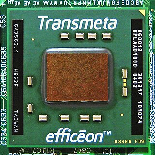
The Efficeon processor is Transmeta's second-generation 256-bit VLIW design released in 2004 which employs a software engine Code Morphing Software (CMS) to convert code written for x86 processors to the native instruction set of the chip. Like its predecessor, the Transmeta Crusoe, Efficeon stresses computational efficiency, low power consumption, and a low thermal footprint.

The AMD Family 10h, or K10, is a microprocessor microarchitecture by AMD based on the K8 microarchitecture. The first third-generation Opteron products for servers were launched on September 10, 2007, with the Phenom processors for desktops following and launching on November 11, 2007 as the immediate successors to the K8 series of processors.

x87 is a floating-point-related subset of the x86 architecture instruction set. It originated as an extension of the 8086 instruction set in the form of optional floating-point coprocessors that work in tandem with corresponding x86 CPUs. These microchips have names ending in "87". This is also known as the NPX. Like other extensions to the basic instruction set, x87 instructions are not strictly needed to construct working programs, but provide hardware and microcode implementations of common numerical tasks, allowing these tasks to be performed much faster than corresponding machine code routines can. The x87 instruction set includes instructions for basic floating-point operations such as addition, subtraction and comparison, but also for more complex numerical operations, such as the computation of the tangent function and its inverse, for example.

<span class="mw-page-title-main">MediaGX</span> Series of x86-compatible processor

The MediaGX CPU is an x86-compatible processor that was designed by Cyrix and manufactured by National Semiconductor following the two companies' merger. It was introduced in 1997. The core is based on the integration of the Cyrix Cx5x86 CPU core with hardware to process video and audio output. Following the buyout of Cyrix by National Semiconductor and the sale of the Cyrix name and trademarks to VIA Technologies, the core was developed by National Semiconductor into the Geode line of processors, which was subsequently sold to Advanced Micro Devices.

<span class="mw-page-title-main">VIA Nano</span>

The VIA Nano is a 64-bit CPU for personal computers. The VIA Nano was released by VIA Technologies in 2008 after five years of development by its CPU division, Centaur Technology. This new Isaiah 64-bit architecture was designed from scratch, unveiled on 24 January 2008, and launched on 29 May, including low-voltage variants and the Nano brand name. The processor supports a number of VIA-specific x86 extensions designed to boost efficiency in low-power appliances.

The Elbrus 2000 is a Russian 512-bit wide VLIW microprocessor developed by Moscow Center of SPARC Technologies (MCST) and fabricated by TSMC.

References

  1. 1 2 Kanellos, Michael; Konrad, Rachel (November 5, 2001). "Transmeta: Are the chips down?". CNET.
  2. "Crusoe - a new world of mobility from Transmeta". 2000-02-29. Archived from the original on 2000-02-29. Retrieved 2023-08-10.
  3. 1 2 3 4 "The Technology Behind Crusoe Processors" (PDF). Washington University in St. Louise SCHOOL OF ENGINEERING AND APPLIED SCIENCE.
  4. 1 2 "TM3120_DataSheet_1-18-00.pdf" (PDF). Transmeta. Archived from the original (PDF) on 2000-08-19. Retrieved 2023-08-10.
  5. 1 2 "TM3200_ProductBrief_5-20-00.pdf" (PDF). Transmeta. Archived from the original (PDF) on 2000-08-18. Retrieved 2023-08-10.
  6. 1 2 3 "TM5400_DataSheet_1-18-00.pdf" (PDF). Archived from the original (PDF) on 2000-08-19.
  7. "tm5400n5600_databook_001101.pdf" (PDF). Transmeta. Archived from the original (PDF) on 2003-12-14. Retrieved 2023-08-10.
  8. "tm5600_productbrief_000802.pdf" (PDF). Transmeta. Archived from the original (PDF) on 2003-12-14. Retrieved 2023-08-10.
  9. 1 2 "Crusoe - a new world of mobility from Transmeta". 2000-11-15. Archived from the original on 2000-11-15. Retrieved 2023-08-10.
  10. "Transmeta Corporation : Crusoe > Specifications > Crusoe TM5500 Processor". 2003-12-11. Archived from the original on 2003-12-11. Retrieved 2023-08-10.
  11. "Transmeta Corporation : Crusoe > Specifications > Crusoe TM5800 Processor". 2003-10-17. Archived from the original on 2003-10-17. Retrieved 2023-08-10.
  12. 1 2 "tmta_processor_comparison.pdf" (PDF). Transmeta. Archived from the original (PDF) on 2005-05-13. Retrieved 2023-08-10.
  13. "embedded_apps_030904.pdf" (PDF). Transmeta. Archived from the original (PDF) on 2003-11-18.
  14. "Transmeta Corporation : Crusoe > Specifications > Crusoe TM5900/TM5700 Processors". 2006-02-14. Archived from the original on 2006-02-14. Retrieved 2023-08-10.
  15. "crusoe_tm5700-tm5900_processor.pdf" (PDF). Transmeta. Archived from the original (PDF) on 2005-05-13. Retrieved 2023-08-10.
  16. Halfhil, Tom R. (February 14, 2000). "Transmeta Breaks x86 Low-Power Barrier" (PDF). Microprocessor Report . Although the FPU/multimedia unit can handle the same data types as Intel's MMX instructions, Crusoe chips don't have the new 128-bit registers defined by Intel's SSE (Streaming SIMD Extensions). Transmeta says Crusoe could emulate SSE-type instructions and registers, but there's not enough software support for SSE to justify the effort at this time.
  17. "Last versions of Windows applications that do not require SSE2 - Matej Horvat". matejhorvat.si. Retrieved 2022-05-16.
  18. "What version of Fire Fox for XP and site to download from? | Firefox Support Forum | Mozilla Support". support.mozilla.org. Retrieved 2022-05-16.
  19. Case, Loy (October 15, 2003). "Transmeta Unveils the Efficeon". ExtremeTech .
  20. "Linux on a Fujitsu P2040". jcl@hunch.net. Retrieved 2022-05-15.
  21. "Thin Clients: HP T5300". Parkytowers.me.uk. Retrieved 2013-07-08.
  22. "HP Thin Client: T5700". Parkytowers.me.uk. Retrieved 2013-07-08.
  23. "Pen Computing Magazine: SONICBlue ProGear". www.pencomputing.com. Retrieved 2020-08-28.
  24. Klaß, Christian (2001-02-16). "Sony Vaio GT1 - Hybrid aus Crusoe-Notebook und DV-Kamera" [Sony Vaio GT1 - hybrid of Crusoe notebook and DV camera]. Golem.de (in German). Retrieved 2024-04-10.

Further reading