Two-dimensional semiconductor

Last updated

A two-dimensional semiconductor (also known as 2D semiconductor) is a type of natural semiconductor with thicknesses on the atomic scale. Geim and Novoselov et al. initiated the field in 2004 when they reported a new semiconducting material graphene, a flat monolayer of carbon atoms arranged in a 2D honeycomb lattice. [1] A 2D monolayer semiconductor is significant because it exhibits stronger piezoelectric coupling than traditionally employed bulk forms. This coupling could enable applications. [2] One research focus is on designing nanoelectronic components by the use of graphene as electrical conductor, hexagonal boron nitride as electrical insulator, and a transition metal dichalcogenide as semiconductor. [3] [4]

Contents

Materials

Monolayer graphene Graphen.jpg
Monolayer graphene

Graphene

Graphene, consisting of single sheets of carbon atoms, has high electron mobility and high thermal conductivity. One issue regarding graphene is its lack of a band gap, which poses a problem in particular with digital electronics because it is unable to switch off field-effect transistors (FETs). [3]

Layered structure of h-BN Boron-nitride-(hexagonal)-side-3D-balls.png
Layered structure of h-BN

Hexagonal boron nitride

Monolayer hexagonal boron nitride (h-BN) is an insulator with a high energy gap (5.97 eV). [5] However, it can also function as a semiconductor with enhanced conductivity due to its zigzag sharp edges and vacancies. h-BN is often used as substrate and barrier due to its insulating property. h-BN also has a large thermal conductivity.

Layered structure of MoS2, Mo in green, S in yellow Molybdenite-3D-balls.png
Layered structure of MoS2, Mo in green, S in yellow

Transition-metal dichalcogenides

Transition-metal dichalcogenide monolayers (TMDs or TMDCs) are a class of two-dimensional materials that have the chemical formula MX2, where M represents transition metals from group VI, V and VI, and X represents a chalcogen such as sulfur, selenium or tellurium. [6] MoS2, MoSe2, MoTe2, WS2 and WSe2 are TMDCs. TMDCs have layered structure with a plane of metal atoms in between two planes of chalcogen atoms as shown in Figure 1. Each layer is bonded strongly in plane, but weakly in interlayers. Therefore, TMDCs can be easily exfoliated into atomically thin layers through various methods. TMDCs show layer-dependent optical and electrical properties. When exfoliated into monolayers, the band gaps of several TMDCs change from indirect to direct, [7] which lead to broad applications in nanoelectronics, [3] optoelectronics, [8] [9] and quantum computing. [10]

III-VI chalcogenides

Another class of 2D semiconductors are III-VI chalcogenides. These materials have the chemical formula MX, where M is a metal from group 13 (Ga, In) and X is a chalcogen atom (S, Se, Te). Typical members of this group are InSe and GaSe, both of which have shown high electronic mobilities and band gaps suitable for a wide range of electronic applications. [11] [12]

Synthesis

CVD setup for MoS2 synthesis CVD setup.PNG
CVD setup for MoS2 synthesis

2D semiconductor materials are often synthesized using a chemical vapor deposition (CVD) method. Because CVD can provide large-area, high-quality, and well-controlled layered growth of 2D semiconductor materials, it also allows synthesis of two-dimensional heterojunctions. [13] When building devices by stacking different 2D materials, mechanical exfoliation followed by transferring is often used. [4] [6] Other possible synthesis methods include electrochemical deposition, [14] [15] chemical exfoliation, hydrothermal synthesis, and thermal decomposition. In 2008 cadmium selenide CdSe quasi 2D platelets were first synthesized by colloidal method with thicknesses of several atomic layers and lateral sizes up to dozens of nanometers. [16] Modification of the procedure allowed to obtain other nanoparticles with different compositions (like CdTe, [17] HgSe, [18] CdSexS1−x alloys, [19] core/shell [20] and core/crown [21] heterostructures) and shapes (as scrolls, [22] nanoribbons, [23] etc).

Mechanical Behavior

2D semiconductor materials unique crystal structures often yield unique mechanical properties, especially in the monolayer limit, such as high stiffness and strength in the 2D atomic plane, but low flexural rigidity. [24] Testing these materials is more challenging that their bulk counterparts, with methods employing the use of scanning probe techniques such as atomic force microscopy (AFM). These experimental methods are typically performed on 2D materials suspended over holes in a substrate. The tip of the AFM is then used to press into the flake and measure the response of the material. From this mechanical properties such as Young modulus, yield strain, and flexural strength.

Graphene

With a Youngs modulus of almost 1 TPa, [25] graphene boasts incredible toughness due to the strength of the carbon-carbon bonding. Graphene however, has a fracture toughness of about 4 MPa/m, making it brittle and easy to crack . [26] Graphene was later shown by the same group that discovered its fracture toughness, to have incredible fore distribution abilities, with about ten times the ability of steel. [27]

Atomically thin boron nitride

Monolayer boron nitride has fracture strength and Youngs modulus of 70.5 GPa and 0.865 TPa, respectively. Boron nitride also maintains its high Youngs modulus and fracture strengths with increasing thickness. [28]

Transition metal dichalcogenides

2D transition metal dichalcogenides are often used in applications such as flexible and stretchable electronics, where an understanding of their mechanical properties and the operational impact of mechanical changes to the materials is paramount for device performance. Under strain TMDs change their electronic bandgap structure of both the direct gap monolayer and the indirect gap few layer cases indicating applied strain as a tunable parameter. [29] Monolayer MoS2 has a Youngs modulus of 270 GPA and with a maximum strain of 10% before yield. [30] In comparison, bilayer MoS2 has a Youngs modulus of 200 GPa attributed to interlayer slip. [30] As layer number is increased further the interlayer slip is overshadowed by the bending rigidity with a Youngs modulus of 330 GPa. [31]

Proposed applications

Proposed TMDC-based high-electron-mobility transistor device with top-gated Schottky contact and TMDC layers with different doping levels. 2D device.PNG
Proposed TMDC-based high-electron-mobility transistor device with top-gated Schottky contact and TMDC layers with different doping levels.

Some applications include electronic devices, [33] photonic and energy harvesting devices, and flexible and transparent substrates. [3] Other applications include on quantum computing qubit devices [10] solar cells, [34] and flexible electronics. [6]

Proposed vdW qubit composed of ZrSe2/SnSe2. The electrode VG applies the vertical electric field, changing the state of the electron in the conduction band, represented by the green Bloch sphere. Zr, Sn, and Se in red, blue, and gray, respectively. VdW qubit.png
Proposed vdW qubit composed of ZrSe2/SnSe2. The electrode VG applies the vertical electric field, changing the state of the electron in the conduction band, represented by the green Bloch sphere. Zr, Sn, and Se in red, blue, and gray, respectively.

Quantum computing

Theoretical work has predicted the control of the band edges hybridization on some van der Waals heterostructures via electric fields and proposed its usage in quantum bit devices, considering the ZrSe2/SnSe2 heterobilayer as an example. [10] Further experimental work has confirmed these predictions for the case of the MoS2/WS2 heterobilayer. [35]

Magnetic NEMS

2D layered magnetic materials are attractive building blocks for nanoelectromechanical systems (NEMS): while they share high stiffness and strength and low mass with other 2D materials, they are magnetically active. Among the large class of newly emerged 2D layered magnetic materials, of particular interest is few-layer CrI3, whose magnetic ground state consists of antiferromagnetically coupled ferromagnetic (FM) monolayers with out-of-plane easy axis. The interlayer exchange interaction is relatively weak, a magnetic field on the order of 0.5 T in the out-of-plane (𝒛) direction can induce spin-flip transition in bilayer CrI3. Remarkable phenomena and device concepts based on detecting and controlling the interlayer magnetic state have been recently demonstrated, including spin-filter giant magnetoresistance, magnetic switching by electric field or electrostatic doping, and spin transistors. The coupling between the magnetic and mechanical properties in atomically thin materials, the basis for 2D magnetic NEMS, however, remains elusive although NEMS made of thicker magnetic materials or coated with FM metals have been studied.

Related Research Articles

<span class="mw-page-title-main">Boron nitride</span> Refractory compound of boron and nitrogen with formula BN

Boron nitride is a thermally and chemically resistant refractory compound of boron and nitrogen with the chemical formula BN. It exists in various crystalline forms that are isoelectronic to a similarly structured carbon lattice. The hexagonal form corresponding to graphite is the most stable and soft among BN polymorphs, and is therefore used as a lubricant and an additive to cosmetic products. The cubic variety analogous to diamond is called c-BN; it is softer than diamond, but its thermal and chemical stability is superior. The rare wurtzite BN modification is similar to lonsdaleite but slightly softer than the cubic form.

<span class="mw-page-title-main">Molybdenum disulfide</span> Chemical compound

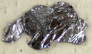
Molybdenum disulfide is an inorganic compound composed of molybdenum and sulfur. Its chemical formula is MoS
2
.

<span class="mw-page-title-main">Epitaxy</span> Crystal growth process relative to the substrate

Epitaxy refers to a type of crystal growth or material deposition in which new crystalline layers are formed with one or more well-defined orientations with respect to the crystalline seed layer. The deposited crystalline film is called an epitaxial film or epitaxial layer. The relative orientation(s) of the epitaxial layer to the seed layer is defined in terms of the orientation of the crystal lattice of each material. For most epitaxial growths, the new layer is usually crystalline and each crystallographic domain of the overlayer must have a well-defined orientation relative to the substrate crystal structure. Epitaxy can involve single-crystal structures, although grain-to-grain epitaxy has been observed in granular films. For most technological applications, single-domain epitaxy, which is the growth of an overlayer crystal with one well-defined orientation with respect to the substrate crystal, is preferred. Epitaxy can also play an important role while growing superlattice structures.

<span class="mw-page-title-main">Graphene</span> Hexagonal lattice made of carbon atoms

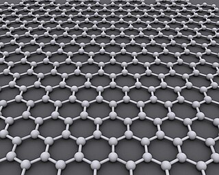
Graphene is an allotrope of carbon consisting of a single layer of atoms arranged in a hexagonal lattice nanostructure. The name is derived from "graphite" and the suffix -ene, reflecting the fact that the graphite allotrope of carbon contains numerous double bonds.

<span class="mw-page-title-main">Tungsten disulfide</span> Chemical compound

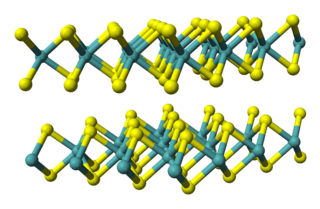
Tungsten disulfide is an inorganic chemical compound composed of tungsten and sulfur with the chemical formula WS2. This compound is part of the group of materials called the transition metal dichalcogenides. It occurs naturally as the rare mineral tungstenite. This material is a component of certain catalysts used for hydrodesulfurization and hydrodenitrification.

<span class="mw-page-title-main">Alex Zettl</span> American nano-scale physicist

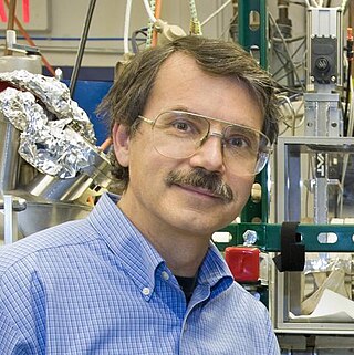
Alex K. Zettl is an American experimental physicist, educator, and inventor.

Piezo-phototronic effect is a three-way coupling effect of piezoelectric, semiconductor and photonic properties in non-central symmetric semiconductor materials, using the piezoelectric potential (piezopotential) that is generated by applying a strain to a semiconductor with piezoelectricity to control the carrier generation, transport, separation and/or recombination at metal–semiconductor junction or p–n junction for improving the performance of optoelectronic devices, such as photodetector, solar cell and light-emitting diode. Prof. Zhong Lin Wang at Georgia Institute of Technology proposed the fundamental principle of this effect in 2010.

<span class="mw-page-title-main">Two-dimensional polymer</span>

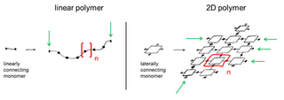
A two-dimensional polymer (2DP) is a sheet-like monomolecular macromolecule consisting of laterally connected repeat units with end groups along all edges. This recent definition of 2DP is based on Hermann Staudinger's polymer concept from the 1920s. According to this, covalent long chain molecules ("Makromoleküle") do exist and are composed of a sequence of linearly connected repeat units and end groups at both termini.

<span class="mw-page-title-main">Tungsten diselenide</span> Chemical compound

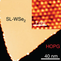
Tungsten diselenide is an inorganic compound with the formula WSe2. The compound adopts a hexagonal crystalline structure similar to molybdenum disulfide. The tungsten atoms are covalently bonded to six selenium ligands in a trigonal prismatic coordination sphere while each selenium is bonded to three tungsten atoms in a pyramidal geometry. The tungsten–selenium bond has a length of 0.2526 nm, and the distance between selenium atoms is 0.334 nm. It is a well studied example of a layered material. The layers stack together via van der Waals interactions. WSe2 is a very stable semiconductor in the group-VI transition metal dichalcogenides.

<span class="mw-page-title-main">Borophene</span> Allotrope of boron

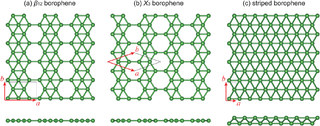
Borophene is a crystalline atomic monolayer of boron, i.e., it is a two-dimensional allotrope of boron and also known as boron sheet. First predicted by theory in the mid-1990s, different borophene structures were experimentally confirmed in 2015.

Valleytronics is an experimental area in semiconductors that exploits local extrema ("valleys") in the electronic band structure. Certain semiconductors have multiple "valleys" in the electronic band structure of the first Brillouin zone, and are known as multivalley semiconductors. Valleytronics is the technology of control over the valley degree of freedom, a local maximum/minimum on the valence/conduction band, of such multivalley semiconductors.

<span class="mw-page-title-main">Transition metal dichalcogenide monolayers</span> Thin semiconductors

Transition-metal dichalcogenide (TMD or TMDC) monolayers are atomically thin semiconductors of the type MX2, with M a transition-metal atom (Mo, W, etc.) and X a chalcogen atom (S, Se, or Te). One layer of M atoms is sandwiched between two layers of X atoms. They are part of the large family of so-called 2D materials, named so to emphasize their extraordinary thinness. For example, a MoS2 monolayer is only 6.5 Å thick. The key feature of these materials is the interaction of large atoms in the 2D structure as compared with first-row transition-metal dichalcogenides, e.g., WTe2 exhibits anomalous giant magnetoresistance and superconductivity.

In materials science, the term single-layer materials or 2D materials refers to crystalline solids consisting of a single layer of atoms. These materials are promising for some applications but remain the focus of research. Single-layer materials derived from single elements generally carry the -ene suffix in their names, e.g. graphene. Single-layer materials that are compounds of two or more elements have -ane or -ide suffixes. 2D materials can generally be categorized as either 2D allotropes of various elements or as compounds.

In materials science, MXenes are a class of two-dimensional inorganic compounds along with MBenes, that consist of atomically thin layers of transition metal carbides, nitrides, or carbonitrides. MXenes accept a variety of hydrophilic terminations. The first MXene was reported in 2011.

Graphene-Boron Nitride nanohybrid materials are a class of compounds created from graphene and boron nitride nanosheets. Graphene and boron nitride both contain intrinsic thermally conductive and electrically insulative properties. The combination of these two compounds may be useful to advance the development and understanding of electronics.

Platinum diselenide is a transition metal dichalcogenide with the formula PtSe2. It is a layered substance that can be split into layers down to three atoms thick. PtSe2 can behave as a metalloid or as a semiconductor depending on the thickness.

<span class="mw-page-title-main">Boron nitride nanosheet</span>

Boron nitride nanosheet is a crystalline form of the hexagonal boron nitride (h-BN), which has a thickness of one atom. Similar in geometry as well as physical and thermal properties to its carbon analog graphene, but has very different chemical and electronic properties – contrary to the black and highly conducting graphene, BN nanosheets are electrical insulators with a band gap of ~5.9 eV, and therefore appear white in color.

Two dimensional hexagonal boron nitride is a material of comparable structure to graphene with potential applications in e.g. photonics., fuel cells and as a substrate for two-dimensional heterostructures. 2D h-BN is isostructural to graphene, but where graphene is conductive, 2D h-BN is a wide-gap insulator.

Tony Frederick Heinz is an American physicist.

<span class="mw-page-title-main">Tantalum diselenide</span> Chemical compound

Tantalum diselenide is a compound made with tantalum and selenium atoms, with chemical formula TaSe2, which belongs to the family of transition metal dichalcogenides. In contrast to molybdenum disulfide (MoS2) or rhenium disulfide (ReS2), tantalum diselenide does not occur spontaneously in nature, but it can be synthesized. Depending on the growth parameters, different types of crystal structures can be stabilized.

References

  1. Novoselov, K. S. (2004). "Electric Field Effect in Atomically Thin Carbon Films". Science. 306 (5696): 666–669. arXiv: cond-mat/0410550 . Bibcode:2004Sci...306..666N. doi:10.1126/science.1102896. ISSN   0036-8075. PMID   15499015. S2CID   5729649.
  2. Song, Xiufeng; Hu, Jinlian; Zeng, Haibo (2013). "Two-dimensional semiconductors: recent progress and future perspectives". Journal of Materials Chemistry C. 1 (17): 2952. doi:10.1039/C3TC00710C.
  3. 1 2 3 4 Radisavljevic, B.; Radenovic, A.; Brivio, J.; Giacometti, V.; Kis, A. (2011). "Single-layer MoS2 transistors". Nature Nanotechnology. 6 (3): 147–150. Bibcode:2011NatNa...6..147R. doi:10.1038/nnano.2010.279. PMID   21278752.
  4. 1 2 Geim, A. K.; Grigorieva, I. V. (2013). "Van der Waals heterostructures". Nature. 499 (7459): 419–425. arXiv: 1307.6718 . doi:10.1038/nature12385. ISSN   0028-0836. PMID   23887427. S2CID   205234832.
  5. Dean, C. R.; Young, A. F.; Meric, I.; Lee, C.; Wang, L.; Sorgenfrei, S.; Watanabe, K.; Taniguchi, T.; Kim, P.; Shepard, K. L.; Hone, J. (2010). "Boron nitride substrates for high-quality graphene electronics". Nature Nanotechnology. 5 (10): 722–726. arXiv: 1005.4917 . Bibcode:2010NatNa...5..722D. doi:10.1038/nnano.2010.172. ISSN   1748-3387. PMID   20729834. S2CID   1493242.
  6. 1 2 3 Wang, Qing Hua; Kalantar-Zadeh, Kourosh; Kis, Andras; Coleman, Jonathan N.; Strano, Michael S. (2012). "Electronics and optoelectronics of two-dimensional transition metal dichalcogenides". Nature Nanotechnology. 7 (11): 699–712. Bibcode:2012NatNa...7..699W. doi:10.1038/nnano.2012.193. ISSN   1748-3387. PMID   23132225. S2CID   6261931.
  7. Kuc, A.; Zibouche, N.; Heine, T. (2011). "Influence of quantum confinement on the electronic structure of the transition metal sulfideTS2". Physical Review B. 83 (24): 245213. arXiv: 1104.3670 . Bibcode:2011PhRvB..83x5213K. doi:10.1103/PhysRevB.83.245213. ISSN   1098-0121. S2CID   119112827.
  8. Wilson, J.A.; Yoffe, A.D. (1969). "The transition metal dichalcogenides discussion and interpretation of the observed optical, electrical and structural properties". Advances in Physics. 18 (73): 193–335. Bibcode:1969AdPhy..18..193W. doi:10.1080/00018736900101307. ISSN   0001-8732.
  9. Yoffe, A D (1973). "Layer Compounds". Annual Review of Materials Science . 3 (1): 147–170. Bibcode:1973AnRMS...3..147Y. doi:10.1146/annurev.ms.03.080173.001051. ISSN   0084-6600.
  10. 1 2 3 4 B. Lucatto; et al. (2019). "Charge qubit in van der Waals heterostructures". Physical Review B. 100 (12): 121406. arXiv: 1904.10785 . Bibcode:2019PhRvB.100l1406L. doi:10.1103/PhysRevB.100.121406. S2CID   129945636.
  11. Arora, Himani; Jung, Younghun; Venanzi, Tommaso; Watanabe, Kenji; Taniguchi, Takashi; Hübner, René; Schneider, Harald; Helm, Manfred; Hone, James C.; Erbe, Artur (2019-11-20). "Effective Hexagonal Boron Nitride Passivation of Few-Layered InSe and GaSe to Enhance Their Electronic and Optical Properties". ACS Applied Materials & Interfaces. 11 (46): 43480–43487. doi:10.1021/acsami.9b13442. hdl: 11573/1555190 . ISSN   1944-8244. PMID   31651146. S2CID   204884014.
  12. Arora, Himani; Erbe, Artur (2021). "Recent progress in contact, mobility, and encapsulation engineering of InSe and GaSe". InfoMat. 3 (6): 662–693. doi: 10.1002/inf2.12160 . ISSN   2567-3165. S2CID   228902032.
  13. Duan, Xidong; Wang, Chen; Shaw, Jonathan C.; Cheng, Rui; Chen, Yu; Li, Honglai; Wu, Xueping; Tang, Ying; Zhang, Qinling; Pan, Anlian; Jiang, Jianhui; Yu, Ruqing; Huang, Yu; Duan, Xiangfeng (2014). "Lateral epitaxial growth of two-dimensional layered semiconductor heterojunctions". Nature Nanotechnology. 9 (12): 1024–1030. Bibcode:2014NatNa...9.1024D. doi:10.1038/nnano.2014.222. ISSN   1748-3387. PMID   25262331.
  14. Noori, Yasir J.; Thomas, Shibin; Ramadan, Sami; Smith, Danielle E.; Greenacre, Vicki K.; Abdelazim, Nema; Han, Yisong; Beanland, Richard; Hector, Andrew L.; Klein, Norbert; Reid, Gillian; Bartlett, Philip N.; Kees de Groot, C. H. (2020-11-04). "Large-Area Electrodeposition of Few-Layer MoS 2 on Graphene for 2D Material Heterostructures". ACS Applied Materials & Interfaces. 12 (44): 49786–49794. arXiv: 2005.08616 . doi:10.1021/acsami.0c14777. ISSN   1944-8244. PMID   33079533. S2CID   224828493.
  15. Noori, Y J; Thomas, S; Ramadan, S; Greenacre, V K; Abdelazim, N M; Han, Y; Zhang, J; Beanland, R; Hector, A L; Klein, N; Reid, G; Bartlett, P N; de Groot, C H (2022-01-01). "Electrodeposited WS 2 monolayers on patterned graphene". 2D Materials. 9 (1): 015025. arXiv: 2109.00083 . Bibcode:2022TDM.....9a5025N. doi:10.1088/2053-1583/ac3dd6. ISSN   2053-1583. S2CID   244693600.
  16. Ithurria, Sandrine; Dubertret, Benoit (2008-12-10). "Quasi 2D Colloidal CdSe Platelets with Thicknesses Controlled at the Atomic Level". Journal of the American Chemical Society. 130 (49): 16504–16505. doi:10.1021/ja807724e. ISSN   0002-7863. PMID   19554725.
  17. Pedetti, Silvia; Nadal, Brice; Lhuillier, Emmanuel; Mahler, Benoit; Bouet, Cécile; Abécassis, Benjamin; Xu, Xiangzhen; Dubertret, Benoit (2013-06-25). "Optimized Synthesis of CdTe Nanoplatelets and Photoresponse of CdTe Nanoplatelets Films". Chemistry of Materials. 25 (12): 2455–2462. doi:10.1021/cm4006844. ISSN   0897-4756. S2CID   101411815.
  18. Izquierdo, Eva; Dufour, Marion; Chu, Audrey; Livache, Clément; Martinez, Bertille; Amelot, Dylan; Patriarche, Gilles; Lequeux, Nicolas; Lhuillier, Emmanuel; Ithurria, Sandrine (2018-06-26). "Coupled HgSe Colloidal Quantum Wells through a Tunable Barrier: A Strategy To Uncouple Optical and Transport Band Gap". Chemistry of Materials. 30 (12): 4065–4072. doi:10.1021/acs.chemmater.8b01028. ISSN   0897-4756. S2CID   103490948.
  19. Fan, Fengjia; Kanjanaboos, Pongsakorn; Saravanapavanantham, Mayuran; Beauregard, Eric; Ingram, Grayson; Yassitepe, Emre; Adachi, Michael M.; Voznyy, Oleksandr; Johnston, Andrew K.; Walters, Grant; Kim, Gi-Hwan (2015-07-08). "Colloidal CdSe1–xSx Nanoplatelets with Narrow and Continuously-Tunable Electroluminescence". Nano Letters. 15 (7): 4611–4615. Bibcode:2015NanoL..15.4611F. doi:10.1021/acs.nanolett.5b01233. ISSN   1530-6984. PMID   26031416.
  20. Mahler, Benoit; Nadal, Brice; Bouet, Cecile; Patriarche, Gilles; Dubertret, Benoit (2012-11-14). "Core/Shell Colloidal Semiconductor Nanoplatelets". Journal of the American Chemical Society. 134 (45): 18591–18598. doi:10.1021/ja307944d. ISSN   0002-7863. PMID   23057684.
  21. Kelestemur, Yusuf; Olutas, Murat; Delikanli, Savas; Guzelturk, Burak; Akgul, Mehmet Zafer; Demir, Hilmi Volkan (2015-01-29). "Type-II Colloidal Quantum Wells: CdSe/CdTe Core/Crown Heteronanoplatelets". The Journal of Physical Chemistry C. 119 (4): 2177–2185. doi:10.1021/jp510466k. hdl: 11693/23136 . ISSN   1932-7447.
  22. Vasiliev, Roman B.; Lazareva, Elizabeth P.; Karlova, Daria A.; Garshev, Alexey V.; Yao, Yuanzhao; Kuroda, Takashi; Gaskov, Alexander M.; Sakoda, Kazuaki (2018-03-13). "Spontaneous Folding of CdTe Nanosheets Induced by Ligand Exchange". Chemistry of Materials. 30 (5): 1710–1717. doi:10.1021/acs.chemmater.7b05324. ISSN   0897-4756.
  23. Deng, Zhengtao; Cao, Di; He, Jin; Lin, Su; Lindsay, Stuart M.; Liu, Yan (2012-07-24). "Solution Synthesis of Ultrathin Single-Crystalline SnS Nanoribbons for Photodetectors via Phase Transition and Surface Processing". ACS Nano. 6 (7): 6197–6207. doi:10.1021/nn302504p. ISSN   1936-0851. PMID   22738287.
  24. Akinwande, D.; Brennan, C. J.; Bunch, J. S.; Egberts, P.; Felts, J. R.; Gao, H.; Huang, R.; Kim, J.-S.; Li, T.; Li, Y.; Liechti, K. M.; Lu, N.; Park, H. S.; Reed, E. J.; Wang, P.; Yakobson, B. I.; Zhang, T.; Zhang, Y.-W.; Zhou, Y.; Zhu, Y. A Review on Mechanics and Mechanical Properties of 2D Materials—Graphene and Beyond. Extreme Mech. Lett.2017, 13, 42–77. https://doi.org/10.1016/j.eml.2017.01.008.
  25. Lee, C.; Wei, X.; Kysar, J. W.; Hone, J. Measurement of the Elastic Properties and Intrinsic Strength of Monolayer Graphene. Science2008, 321 (5887), 385–388. https://doi.org/10.1126/science.1157996.
  26. Zhang, P.; Ma, L.; Fan, F.; Zeng, Z.; Peng, C.; Loya, P. E.; Liu, Z.; Gong, Y.; Zhang, J.; Zhang, X.; Ajayan, P. M.; Zhu, T.; Lou, J. Fracture Toughness of Graphene. Nat. Commun.2014, 5 (1), 3782. https://doi.org/10.1038/ncomms4782.
  27. Dorrieron, Jason (4 December 2014). "Graphene Armor Would Be Light, Flexible and Far Stronger Than Steel". Singularity Hub. Retrieved 6 October 2016.
  28. Falin, A.; Cai, Q.; Santos, E. J. G.; Scullion, D.; Qian, D.; Zhang, R.; Yang, Z.; Huang, S.; Watanabe, K.; Taniguchi, T.; Barnett, M. R.; Chen, Y.; Ruoff, R. S.; Li, L. H. Mechanical Properties of Atomically Thin Boron Nitride and the Role of Interlayer Interactions. Nat. Commun.2017, 8, 15815. https://doi.org/10.1038/ncomms15815.
  29. Conley, H. J.; Wang, B.; Ziegler, J. I.; Haglund Jr., R. F.; Pantelides, S. T.; Bolotin, K. I. Bandgap Engineering of Strained Monolayer and Bilayer MoS2. Nano Lett.2013, 13 (8), 3626–3630. https://doi.org/10.1021/nl4014748.
  30. 1 2 Bertolazzi, S.; Brivio, J.; Kis, A. Stretching and Breaking of Ultrathin MoS2. ACS Nano2011, 5 (12), 9703–9709. https://doi.org/10.1021/nn203879f.
  31. Castellanos-Gomez, A.; Poot, M.; Steele, G. A.; van der Zant, H. S. J.; Agraït, N.; Rubio-Bollinger, G. Elastic Properties of Freely Suspended MoS2 Nanosheets. Adv. Mater.2012, 24 (6), 772–775. https://doi.org/10.1002/adma.201103965.
  32. Ong, Zhun-Yong; Bae, Myung-Ho (2019). "Energy dissipation in van der Waals 2D devices". 2D Materials. 6 (3): 032005. arXiv: 1904.09752 . Bibcode:2019TDM.....6c2005O. doi:10.1088/2053-1583/ab20ea. S2CID   128345575.
  33. McClellan, Connor. "Stanford 2D Device Trends".
  34. Shanmugam, Mariyappan; Jacobs-Gedrim, Robin; Song, Eui Sang; Yu, Bin (2014). "Two-dimensional layered semiconductor/graphene heterostructures for solar photovoltaic applications". Nanoscale. 6 (21): 12682–12689. Bibcode:2014Nanos...612682S. doi:10.1039/C4NR03334E. ISSN   2040-3364. PMID   25210837.
  35. Kiemle, Jonas; et al. (2020). "Control of the orbital character of indirect excitons in MoS2/WS2 heterobilayers". Phys. Rev. B. 101 (12): 121404. arXiv: 1912.02479 . Bibcode:2020PhRvB.101l1404K. doi:10.1103/PhysRevB.101.121404. S2CID   208637170.