Related Research Articles
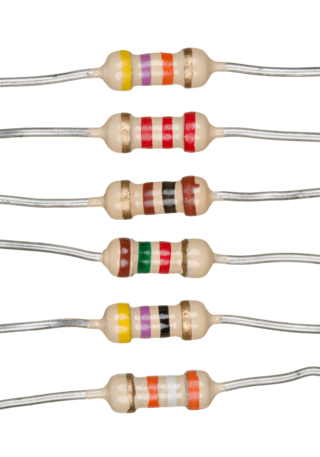
A resistor is a passive two-terminal electrical component that implements electrical resistance as a circuit element. In electronic circuits, resistors are used to reduce current flow, adjust signal levels, to divide voltages, bias active elements, and terminate transmission lines, among other uses. High-power resistors that can dissipate many watts of electrical power as heat may be used as part of motor controls, in power distribution systems, or as test loads for generators. Fixed resistors have resistances that only change slightly with temperature, time or operating voltage. Variable resistors can be used to adjust circuit elements, or as sensing devices for heat, light, humidity, force, or chemical activity.

In microelectronics, a dual in-line package is an electronic component package with a rectangular housing and two parallel rows of electrical connecting pins. The package may be through-hole mounted to a printed circuit board (PCB) or inserted in a socket. The dual-inline format was invented by Don Forbes, Rex Rice and Bryant Rogers at Fairchild R&D in 1964, when the restricted number of leads available on circular transistor-style packages became a limitation in the use of integrated circuits. Increasingly complex circuits required more signal and power supply leads ; eventually microprocessors and similar complex devices required more leads than could be put on a DIP package, leading to development of higher-density chip carriers. Furthermore, square and rectangular packages made it easier to route printed-circuit traces beneath the packages.
In electrical engineering, a ground plane is an electrically conductive surface, usually connected to electrical ground.

A printed circuit board (PCB), also called printed wiring board (PWB), is a medium used to connect or "wire" components to one another in a circuit. It takes the form of a laminated sandwich structure of conductive and insulating layers: each of the conductive layers is designed with a pattern of traces, planes and other features etched from one or more sheet layers of copper laminated onto and/or between sheet layers of a non-conductive substrate. Electrical components may be fixed to conductive pads on the outer layers in the shape designed to accept the component's terminals, generally by means of soldering, to both electrically connect and mechanically fasten them to it. Another manufacturing process adds vias, plated-through holes that allow interconnections between layers.

In electronics, point-to-point construction is a non-automated technique for constructing circuits which was widely used before the use of printed circuit boards (PCBs) and automated assembly gradually became widespread following their introduction in the 1950s. Circuits using thermionic valves were relatively large, relatively simple, and used large sockets, all of which made the PCB less obviously advantageous than with later complex semiconductor circuits. Point-to-point construction is still widespread in power electronics, where components are bulky and serviceability is a consideration, and to construct prototype equipment with few or heavy electronic components. A common practice, especially in older point-to-point construction, is to use the leads of components such as resistors and capacitors to bridge as much of the distance between connections as possible, reducing the need to add additional wire between the components.

A breadboard, solderless breadboard, or protoboard is a construction base used to build semi-permanent prototypes of electronic circuits. Unlike a perfboard or stripboard, breadboards do not require soldering or destruction of tracks and are hence reusable. For this reason, breadboards are also popular with students and in technological education.

Components of an electrical circuit are electrically connected if an electric current can run between them through an electrical conductor. An electrical connector is an electromechanical device used to create an electrical connection between parts of an electrical circuit, or between different electrical circuits, thereby joining them into a larger circuit.

A ball grid array (BGA) is a type of surface-mount packaging used for integrated circuits. BGA packages are used to permanently mount devices such as microprocessors. A BGA can provide more interconnection pins than can be put on a dual in-line or flat package. The whole bottom surface of the device can be used, instead of just the perimeter. The traces connecting the package's leads to the wires or balls which connect the die to package are also on average shorter than with a perimeter-only type, leading to better performance at high speeds.

Stripboard is the generic name for a widely used type of electronics prototyping material for circuit boards characterized by a pre-formed 0.1 inches (2.54 mm) regular (rectangular) grid of holes, with wide parallel strips of copper cladding running in one direction all the way along one side of an insulating bonded paper board. It is commonly also known by the name of the original product Veroboard, which is a trademark, in the UK, of British company Vero Technologies Ltd and Canadian company Pixel Print Ltd. It was originated and developed in the early 1960s by the Electronics Department of Vero Precision Engineering Ltd (VPE). It was introduced as a general-purpose material for use in constructing electronic circuits - differing from purpose-designed printed circuit boards (PCBs) in that a variety of electronics circuits may be constructed using a standard wiring board.

Flip chip, also known as controlled collapse chip connection or its abbreviation, C4, is a method for interconnecting dies such as semiconductor devices, IC chips, integrated passive devices and microelectromechanical systems (MEMS), to external circuitry with solder bumps that have been deposited onto the chip pads. The technique was developed by General Electric's Light Military Electronics Department, Utica, New York. The solder bumps are deposited on the chip pads on the top side of the wafer during the final wafer processing step. In order to mount the chip to external circuitry, it is flipped over so that its top side faces down, and aligned so that its pads align with matching pads on the external circuit, and then the solder is reflowed to complete the interconnect. This is in contrast to wire bonding, in which the chip is mounted upright and fine wires are welded onto the chip pads and lead frame contacts to interconnect the chip pads to external circuitry.

The D-subminiature or D-sub is a common type of electrical connector. They are named for their characteristic D-shaped metal shield. When they were introduced, D-subs were among the smallest connectors used on computer systems.

Integrated circuit packaging is the final stage of semiconductor device fabrication, in which the die is encapsulated in a supporting case that prevents physical damage and corrosion. The case, known as a "package", supports the electrical contacts which connect the device to a circuit board.

In electronics, through-hole technology is a manufacturing scheme in which leads on the components are inserted through holes drilled in printed circuit boards (PCB) and soldered to pads on the opposite side, either by manual assembly or by the use of automated insertion mount machines.
A via is an electrical connection between two or more metal layers of a printed circuit boards (PCB) or integrated circuit. Essentially a via is a small drilled hole that goes through two or more adjacent layers; the hole is plated with metal that forms an electrical connection through the insulating layers.
Conformal coating is a protective, breathable coating of thin polymeric film applied to printed circuit boards (PCBs). Conformal coatings are typically applied at 25–250 μm to the electronic circuitry and protect against moisture and other severe conditions.
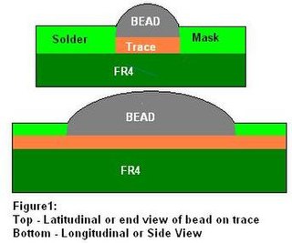
Bead probe technology (BPT) is technique used to provide electrical access to printed circuit board (PCB) circuitry for performing in-circuit testing (ICT). It makes use of small beads of solder placed onto the board's traces to allow measuring and controlling of the signals using a test probe. This permits test access to boards on which standard ICT test pads are not feasible due to space constraints.

Elastomeric connectors, also known by the registered trademark ZEBRA connectors, consist of alternating conductive and insulating regions in a rubber or elastomer matrix to produce overall anisotropic conductive properties. The original version consisted of alternating conductive and insulating layers of silicone rubber, cut crosswise to expose the thin layers. They provide high-density redundant electrical paths for high reliability connections. One of the first applications was connecting thin and fragile glass liquid-crystal displays (LCDs) to circuit boards in electronic devices, as little current was required.

A pin header is a form of electrical connector. A male pin header consists of one or more rows of metal pins molded into a plastic base, often 2.54 mm (0.1 in) apart, though available in many spacings. Male pin headers are cost-effective due to their simplicity. The female counterparts are sometimes known as female headers, though there are numerous naming variations of male and female connectors. Historically, headers have sometimes been called "Berg connectors" or "DuPont" connectors, but headers are manufactured by many companies.
References
- ↑ http://www.we-online.de/web/de/intelligente_systeme/neu__skedd/startseite.php. 2015-08-26.
- ↑ "RZ Series". www.airborn.com. Retrieved 2018-08-22.