
Double Data Rate Synchronous Dynamic Random-Access Memory is a double data rate (DDR) synchronous dynamic random-access memory (SDRAM) class of memory integrated circuits used in computers. DDR SDRAM, also retroactively called DDR1 SDRAM, has been superseded by DDR2 SDRAM, DDR3 SDRAM, DDR4 SDRAM and DDR5 SDRAM. None of its successors are forward or backward compatible with DDR1 SDRAM, meaning DDR2, DDR3, DDR4 and DDR5 memory modules will not work on DDR1-equipped motherboards, and vice versa.

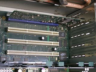
Peripheral Component Interconnect (PCI) is a local computer bus for attaching hardware devices in a computer and is part of the PCI Local Bus standard. The PCI bus supports the functions found on a processor bus but in a standardized format that is independent of any given processor's native bus. Devices connected to the PCI bus appear to a bus master to be connected directly to its own bus and are assigned addresses in the processor's address space. It is a parallel bus, synchronous to a single bus clock. Attached devices can take either the form of an integrated circuit fitted onto the motherboard or an expansion card that fits into a slot. The PCI Local Bus was first implemented in IBM PC compatibles, where it displaced the combination of several slow Industry Standard Architecture (ISA) slots and one fast VESA Local Bus (VLB) slot as the bus configuration. It has subsequently been adopted for other computer types. Typical PCI cards used in PCs include: network cards, sound cards, modems, extra ports such as Universal Serial Bus (USB) or serial, TV tuner cards and hard disk drive host adapters. PCI video cards replaced ISA and VLB cards until rising bandwidth needs outgrew the abilities of PCI. The preferred interface for video cards then became Accelerated Graphics Port (AGP), a superset of PCI, before giving way to PCI Express.
Direct memory access (DMA) is a feature of computer systems that allows certain hardware subsystems to access main system memory independently of the central processing unit (CPU).

Dynamic random-access memory is a type of random-access semiconductor memory that stores each bit of data in a memory cell, usually consisting of a tiny capacitor and a transistor, both typically based on metal–oxide–semiconductor (MOS) technology. While most DRAM memory cell designs use a capacitor and transistor, some only use two transistors. In the designs where a capacitor is used, the capacitor can either be charged or discharged; these two states are taken to represent the two values of a bit, conventionally called 0 and 1. The electric charge on the capacitors gradually leaks away; without intervention the data on the capacitor would soon be lost. To prevent this, DRAM requires an external memory refresh circuit which periodically rewrites the data in the capacitors, restoring them to their original charge. This refresh process is the defining characteristic of dynamic random-access memory, in contrast to static random-access memory (SRAM) which does not require data to be refreshed. Unlike flash memory, DRAM is volatile memory, since it loses its data quickly when power is removed. However, DRAM does exhibit limited data remanence.

Synchronous dynamic random-access memory is any DRAM where the operation of its external pin interface is coordinated by an externally supplied clock signal.
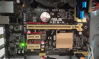
PCI Express, officially abbreviated as PCIe or PCI-e, is a high-speed serial computer expansion bus standard, designed to replace the older PCI, PCI-X and AGP bus standards. It is the common motherboard interface for personal computers' graphics cards, sound cards, hard disk drive host adapters, SSDs, Wi-Fi and Ethernet hardware connections. PCIe has numerous improvements over the older standards, including higher maximum system bus throughput, lower I/O pin count and smaller physical footprint, better performance scaling for bus devices, a more detailed error detection and reporting mechanism, and native hot-swap functionality. More recent revisions of the PCIe standard provide hardware support for I/O virtualization.

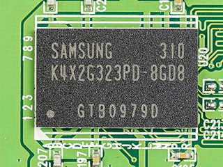
Double Data Rate 2 Synchronous Dynamic Random-Access Memory is a double data rate (DDR) synchronous dynamic random-access memory (SDRAM) interface. It is a JEDEC standard (JESD79-2); first published in September 2003. DDR2 succeeded the original DDR SDRAM specification, and was itself succeeded by DDR3 SDRAM in 2007. DDR2 DIMMs are neither forward compatible with DDR3 nor backward compatible with DDR.
PCI-X, short for Peripheral Component Interconnect eXtended, is a computer bus and expansion card standard that enhances the 32-bit PCI local bus for higher bandwidth demanded mostly by servers and workstations. It uses a modified protocol to support higher clock speeds, but is otherwise similar in electrical implementation. PCI-X 2.0 added speeds up to 533 MHz, with a reduction in electrical signal levels.

In computing, double data rate (DDR) describes a computer bus that transfers data on both the rising and falling edges of the clock signal and hence doubles the memory bandwidth by transferring data twice per clock cycle. This is also known as double pumped, dual-pumped, and double transition. The term toggle mode is used in the context of NAND flash memory.
XDR DRAM is a high-performance dynamic random-access memory interface. It is based on and succeeds RDRAM. Competing technologies include DDR2 and GDDR4.

The Low Pin Count (LPC) bus is a computer bus used on IBM-compatible personal computers to connect low-bandwidth devices to the CPU, such as the BIOS ROM, "legacy" I/O devices, and Trusted Platform Module (TPM). "Legacy" I/O devices usually include serial and parallel ports, PS/2 keyboard, PS/2 mouse, and floppy disk controller.
Double Data Rate 3 Synchronous Dynamic Random-Access Memory is a type of synchronous dynamic random-access memory (SDRAM) with a high bandwidth interface, and has been in use since 2007. It is the higher-speed successor to DDR and DDR2 and predecessor to DDR4 synchronous dynamic random-access memory (SDRAM) chips. DDR3 SDRAM is neither forward nor backward compatible with any earlier type of random-access memory (RAM) because of different signaling voltages, timings, and other factors.
GIO is a computer bus standard developed by SGI and used in a variety of their products in the 1990s as their primary expansion system. GIO was similar in concept to competing standards such as NuBus or (later) PCI, but saw little use outside SGI and severely limited the devices available on their platform as a result. Most devices using GIO were SGI's own graphics cards, although a number of cards supporting high-speed data access such as Fibre Channel and FDDI were available from third parties. Later SGI machines use the XIO bus, which is laid out as a computer network as opposed to a bus.
Released as the expansion bus of the Commodore Amiga 3000 in 1990, the Zorro III computer bus was used to attach peripheral devices to an Amiga motherboard. Designed by Commodore International lead engineer Dave Haynie, the 32-bit Zorro III replaced the 16-bit Zorro II bus used in the Amiga 2000. As with the Zorro II bus, Zorro III allowed for true Plug and Play autodetection wherein devices were dynamically allocated the resources they needed on boot.
Memory bandwidth is the rate at which data can be read from or stored into a semiconductor memory by a processor. Memory bandwidth is usually expressed in units of bytes/second, though this can vary for systems with natural data sizes that are not a multiple of the commonly used 8-bit bytes.
Message Signaled Interrupts (MSI) are a method of signaling interrupts, using special in-band messages to replace traditional out-of-band signals on dedicated interrupt lines. While message signaled interrupts are more complex to implement in a device, they have some significant advantages over pin-based out-of-band interrupt signalling, such as improved interrupt handling performance. This is in contrast to traditional interrupt mechanisms, such as the legacy interrupt request (IRQ) system.
Low-Power Double Data Rate (LPDDR), also known as LPDDR SDRAM, is a type of synchronous dynamic random-access memory that consumes less power and is targeted for mobile computers and devices such as mobile phones. Older variants are also known as Mobile DDR, and abbreviated as mDDR.

GDDR3 SDRAM is a type of DDR SDRAM specialized for graphics processing units (GPUs) offering less access latency and greater device bandwidths. Its specification was developed by ATI Technologies in collaboration with DRAM vendors including Elpida Memory, Hynix Semiconductor, Infineon and Micron. It was later adopted as a JEDEC standard.
Compute Express Link (CXL) is an open standard for high-speed, high capacity central processing unit (CPU)-to-device and CPU-to-memory connections, designed for high performance data center computers. CXL is built on the serial PCI Express (PCIe) physical and electrical interface and includes PCIe-based block input/output protocol (CXL.io) and new cache-coherent protocols for accessing system memory (CXL.cache) and device memory (CXL.mem). The serial communication and pooling capabilities allows CXL memory to overcome performance and socket packaging limitations of common DIMM memory when implementing high storage capacities.
