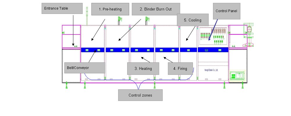
A conveyor belt furnace is a furnace that uses a conveyor or belt to carry process parts or material through a primary heating chamber for rapid thermal processing. It is designed for fast drying and curing of products, and has widespread use in the firing process of thick film and metallization process of solar cell manufacturing. Other names for conveyor belt furnace include metallization furnace, belt furnace, atmosphere furnace, infrared furnace and fast fire furnace.
Conveyor furnaces typically adopt a tunnel structure and contain multiple controlled zones including preheating, binder burn out, heating, firing, and cooling. A conveyor furnace also features fast thermal responses, uniform and stable temperature distribution. Some can heat treated parts to around 1050 °C. The belt speed of a conveyor furnace can be as high as to 6000 mm/min. Products are heated efficiently by infrared radiation (a furnace can also use ceramic heaters or IR lamps) and are dried and fired after passing through the controlled zones, followed by rapid cooling.
After a paste is screened onto a substrate and it settles for 5–15 minutes at room temperature, it undergoes oven drying at 100-150 °C for 10–15 minutes to remove solvents. Firing is then completed in conveyor belt furnaces at temperatures between 500 and 1000 °C.
Electrical contacts are usually formed by screen printing. The firing is done in conveyor belt furnaces at a temperature of about 700 °C for a few minutes. Upon firing, the organic solvents evaporate and the metal powder becomes a conducting path for the electric current.
A transparent conducting glass, coated with doped SnO2 or ITO film, is used as a substrate. A thin film, such as CdS, is then deposited through CSS or CBD techniques. The CdS film is heat treated by a conveyor belt furnace in a reducing atmosphere or in the presence of CdCl2 at 400-500 °C.
TiO2 nanoparticles have been used extensively to increase the interfacial surface area in dye-sensitized solar cells. Nanoparticle films are generally made by screen printing a paste of titania nanocrystals and then sintering the particles together at 450-500 °C in a conveyor belt furnace.
Chemical vapor deposition (CVD) is a vacuum deposition method used to produce high-quality, and high-performance, solid materials. The process is often used in the semiconductor industry to produce thin films.
Surface-mount technology (SMT), originally called planar mounting, is a method in which the electrical components are mounted directly onto the surface of a printed circuit board (PCB). An electrical component mounted in this manner is referred to as a surface-mount device (SMD). In industry, this approach has largely replaced the through-hole technology construction method of fitting components, in large part because SMT allows for increased manufacturing automation which reduces cost and improves quality. It also allows for more components to fit on a given area of substrate. Both technologies can be used on the same board, with the through-hole technology often used for components not suitable for surface mounting such as large transformers and heat-sinked power semiconductors.
Brazing is a metal-joining process in which two or more metal items are joined by melting and flowing a filler metal into the joint, with the filler metal having a lower melting point than the adjoining metal.
In materials science, a refractory is a material that is resistant to decomposition by heat or chemical attack that retains its strength and rigidity at high temperatures. They are inorganic, non-metallic compounds that may be porous or non-porous, and their crystallinity varies widely: they may be crystalline, polycrystalline, amorphous, or composite. They are typically composed of oxides, carbides or nitrides of the following elements: silicon, aluminium, magnesium, calcium, boron, chromium and zirconium. Many refractories are ceramics, but some such as graphite are not, and some ceramics such as clay pottery are not considered refractory. Refractories are distinguished from the refractory metals, which are elemental metals and their alloys that have high melting temperatures.
A heating element is a device used for conversion of electric energy into heat, consisting of a heating resistor and accessories. Heat is generated by the passage of electric current through a resistor through a process known as Joule Heating. Heating elements are used in household appliances, industrial equipment, and scientific instruments enabling them to perform tasks such as cooking, warming, or maintaining specific temperatures higher than the ambient.
Reflow soldering is a process in which a solder paste is used to temporarily attach anywhere from one to thousands of tiny electrical components to their contact pads, after which the entire assembly is subjected to controlled heat. The solder paste reflows in a molten state, creating permanent solder joints. Heating may be accomplished by passing the assembly through a reflow oven, under an infrared lamp, or by soldering individual joints with a hot air pencil.
In materials science, the sol–gel process is a method for producing solid materials from small molecules. The method is used for the fabrication of metal oxides, especially the oxides of silicon (Si) and titanium (Ti). The process involves conversion of monomers in solution into a colloidal solution (sol) that acts as the precursor for an integrated network of either discrete particles or network polymers. Typical precursors are metal alkoxides. Sol–gel process is used to produce ceramic nanoparticles.
Microwave chemistry is the science of applying microwave radiation to chemical reactions. Microwaves act as high frequency electric fields and will generally heat any material containing mobile electric charges, such as polar molecules in a solvent or conducting ions in a solid. Polar solvents are heated as their component molecules are forced to rotate with the field and lose energy in collisions. Semiconducting and conducting samples heat when ions or electrons within them form an electric current and energy is lost due to the electrical resistance of the material. Microwave heating in the laboratory began to gain wide acceptance following papers in 1986, although the use of microwave heating in chemical modification can be traced back to the 1950s. Although occasionally known by such acronyms as MAOS, MEC or MORE synthesis, these acronyms have had little acceptance outside a small number of groups.
Rapid thermal processing (RTP) is a semiconductor manufacturing process which heats silicon wafers to temperatures exceeding 1,000°C for not more than a few seconds. During cooling wafer temperatures must be brought down slowly to prevent dislocations and wafer breakage due to thermal shock. Such rapid heating rates are often attained by high intensity lamps or lasers. These processes are used for a wide variety of applications in semiconductor manufacturing including dopant activation, thermal oxidation, metal reflow and chemical vapor deposition.
An infrared thermometer is a thermometer which infers temperature from a portion of the thermal radiation sometimes called black-body radiation emitted by the object being measured. They are sometimes called laser thermometers as a laser is used to help aim the thermometer, or non-contact thermometers or temperature guns, to describe the device's ability to measure temperature from a distance. By knowing the amount of infrared energy emitted by the object and its emissivity, the object's temperature can often be determined within a certain range of its actual temperature. Infrared thermometers are a subset of devices known as "thermal radiation thermometers".
Dip coating is an industrial coating process which is used, for example, to manufacture bulk products such as coated fabrics and condoms and specialised coatings for example in the biomedical field. Dip coating is also commonly used in academic research, where many chemical and nano material engineering research projects use the dip coating technique to create thin-film coatings.
Germanium telluride (GeTe) is a chemical compound of germanium and tellurium and is a component of chalcogenide glass. It shows semimetallic conduction and ferroelectric behaviour.
For environmental remediation, Low-temperature thermal desorption (LTTD), also known as low-temperature thermal volatilization, thermal stripping, and soil roasting, is an ex-situ remedial technology that uses heat to physically separate petroleum hydrocarbons from excavated soils. Thermal desorbers are designed to heat soils to temperatures sufficient to cause constituents to volatilize and desorb from the soil. Although they are not designed to decompose organic constituents, thermal desorbers can, depending upon the specific organics present and the temperature of the desorber system, cause some organic constituents to completely or partially decompose. The vaporized hydrocarbons are generally treated in a secondary treatment unit prior to discharge to the atmosphere. Afterburners and oxidizers destroy the organic constituents. Condensers and carbon adsorption units trap organic compounds for subsequent treatment or disposal.
An infrared heater or heat lamp is a heating appliance containing a high-temperature emitter that transfers energy to a cooler object through electromagnetic radiation. Depending on the temperature of the emitter, the wavelength of the peak of the infrared radiation ranges from 750 nm to 1 mm. No contact or medium between the emitter and cool object is needed for the energy transfer. Infrared heaters can be operated in vacuum or atmosphere.
Thick-film technology is used to produce electronic devices/modules such as surface mount devices modules, hybrid integrated circuits, heating elements, integrated passive devices and sensors. Main manufacturing technique is screen printing (stenciling), which in addition to use in manufacturing electronic devices can also be used for various graphic reproduction targets. It became one of the key manufacturing/miniaturisation techniques of electronic devices/modules during 1950s. Typical film thickness – manufactured with thick film manufacturing processes for electronic devices – is 0.0001 to 0.1 mm.
A copper indium gallium selenide solar cell is a thin-film solar cell used to convert sunlight into electric power. It is manufactured by depositing a thin layer of copper indium gallium selenide solid solution on glass or plastic backing, along with electrodes on the front and back to collect current. Because the material has a high absorption coefficient and strongly absorbs sunlight, a much thinner film is required than of other semiconductor materials.
Ultra-high-purity steam, also called the clean steam, UHP steam or high purity water vapor, is used in a variety of industrial manufacturing processes that require oxidation or annealing. These processes include the growth of oxide layers on silicon wafers for the semiconductor industry, originally described by the Deal-Grove model, and for the formation of passivation layers used to improve the light capture ability of crystalline photovoltaic cells. Several methods and technologies can be employed to generate ultra high purity steam, including pyrolysis, bubbling, direct liquid injection, and purified steam generation. The level of purity, or the relative lack of contamination, affects the quality of the oxide layer or annealed surface. The method of delivery affects growth rate, uniformity, and electrical performance. Oxidation and annealing are common steps in the manufacture of such devices as microelectronics and solar cells.
Glass frit bonding, also referred to as glass soldering or seal glass bonding, describes a wafer bonding technique with an intermediate glass layer. It is a widely used encapsulation technology for surface micro-machined structures, e.g., accelerometers or gyroscopes. This technique utilizes low melting-point glass and therefore provides various advantages including that viscosity of glass decreases with an increase of temperature. The viscous flow of glass has effects to compensate and planarize surface irregularities, convenient for bonding wafers with a high roughness due to plasma etching or deposition. A low viscosity promotes hermetically sealed encapsulation of structures based on a better adaption of the structured shapes. Further, the coefficient of thermal expansion (CTE) of the glass material is adapted to silicon. This results in low stress in the bonded wafer pair. The glass has to flow and wet the soldered surfaces well below the temperature where deformation or degradation of either of the joined materials or nearby structures occurs. The usual temperature of achieving flowing and wetting is between 450 and 550 °C.
A belt dryer a kind of industrial dryer, is an apparatus which is used for continuous drying and cooling of woodchip, pellets, pastes, moulded compounds and panels using air, inert gas, or flue gas.
Photonic curing is the high-temperature thermal processing of a thin film using pulsed light from a flashlamp. When this transient processing is done on a low-temperature substrate such as plastic or paper, it is possible to attain a significantly higher temperature than the substrate can ordinarily withstand under an equilibrium heating source such as an oven. Since the rate of most thermal curing processes generally increase exponentially with temperature, this process allows materials to be cured much more rapidly than with an oven.