
A scanning electron microscope (SEM) is a type of electron microscope that produces images of a sample by scanning the surface with a focused beam of electrons. The electrons interact with atoms in the sample, producing various signals that contain information about the surface topography and composition of the sample. The electron beam is scanned in a raster scan pattern, and the position of the beam is combined with the intensity of the detected signal to produce an image. In the most common SEM mode, secondary electrons emitted by atoms excited by the electron beam are detected using a secondary electron detector. The number of secondary electrons that can be detected, and thus the signal intensity, depends, among other things, on specimen topography. Some SEMs can achieve resolutions better than 1 nanometer.
Scanning probe microscopy (SPM) is a branch of microscopy that forms images of surfaces using a physical probe that scans the specimen. SPM was founded in 1981, with the invention of the scanning tunneling microscope, an instrument for imaging surfaces at the atomic level. The first successful scanning tunneling microscope experiment was done by Gerd Binnig and Heinrich Rohrer. The key to their success was using a feedback loop to regulate gap distance between the sample and the probe.

Surface roughness can be regarded as the quality of a surface of not being smooth and it is hence linked to human (haptic) perception of the surface texture. From a mathematical perspective it is related to the spatial variability structure of surfaces, and inherently it is a multiscale property. It has different interpretations and definitions depending on the disciplines considered.
Surface metrology is the measurement of small-scale features on surfaces, and is a branch of metrology. Surface primary form, surface fractality, and surface finish are the parameters most commonly associated with the field. It is important to many disciplines and is mostly known for the machining of precision parts and assemblies which contain mating surfaces or which must operate with high internal pressures.

A profilometer is a measuring instrument used to measure a surface's profile, in order to quantify its roughness. Critical dimensions as step, curvature, flatness are computed from the surface topography.

Focused ion beam, also known as FIB, is a technique used particularly in the semiconductor industry, materials science and increasingly in the biological field for site-specific analysis, deposition, and ablation of materials. A FIB setup is a scientific instrument that resembles a scanning electron microscope (SEM). However, while the SEM uses a focused beam of electrons to image the sample in the chamber, a FIB setup uses a focused beam of ions instead. FIB can also be incorporated in a system with both electron and ion beam columns, allowing the same feature to be investigated using either of the beams. FIB should not be confused with using a beam of focused ions for direct write lithography. These are generally quite different systems where the material is modified by other mechanisms.
KLA Corporation is an American capital equipment company based in Milpitas, California. It supplies process control and yield management systems for the semiconductor industry and other related nanoelectronics industries. The company's products and services are intended for all phases of wafer, reticle, integrated circuit (IC) and packaging production, from research and development to final volume manufacturing.

Jenoptik AG is a Jena, Germany-based integrated photonics company. The company is listed on the Frankfurt Stock Exchange and is included in the TecDAX stock index.
ISO 25178: Geometrical Product Specifications (GPS) – Surface texture: areal is an International Organization for Standardization collection of international standards relating to the analysis of 3D areal surface texture.
Bioimage informatics is a subfield of bioinformatics and computational biology. It focuses on the use of computational techniques to analyze bioimages, especially cellular and molecular images, at large scale and high throughput. The goal is to obtain useful knowledge out of complicated and heterogeneous image and related metadata.
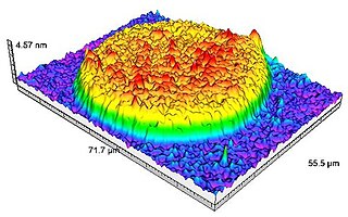
Focus variation is a method used to sharpen images and to measure surface irregularities by means of optics with limited depth of field.
Sarfus is an optical quantitative imaging technique based on the association of:

Leica Microsystems GmbH is a German microscope manufacturing company. It is a manufacturer of optical microscopes, equipment for the preparation of microscopic specimens and related products. There are ten plants in eight countries with distribution partners in over 100 countries. Leica Microsystems emerged in 1997 out of a 1990 merger between Wild-Leitz, headquartered in Heerbrugg Switzerland, and Cambridge Instruments of Cambridge England. The merger of those two umbrella companies created an alliance of the following 8 individual manufacturers of scientific instruments. American Optical Scientific Products, Carl Reichert Optische Werke AG, R.Jung, Bausch and Lomb Optical Scientific Products Division, Cambridge Instruments, E.Leitz Wetzlar, Kern & Co., and Wild Heerbrugg AG, bringing much-needed modernization and a broader degree of expertise to the newly created entity called Leica Holding B.V. group. In 1997 the name was changed to Leica Microsystems and is a wholly-owned entity of Danaher Corporation since July 2005. Danaher is a US venture capital company.
Nikon Instruments is a division of Nikon Corporation, which is headquartered in Tokyo. Its US operations are based in Melville, New York and its European operations in Amstelveen, Netherlands. Nikon Instruments is a specialist in optical instrumentation.
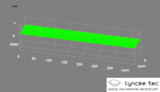
Digital holographic microscopy (DHM) is digital holography applied to microscopy. Digital holographic microscopy distinguishes itself from other microscopy methods by not recording the projected image of the object. Instead, the light wave front information originating from the object is digitally recorded as a hologram, from which a computer calculates the object image by using a numerical reconstruction algorithm. The image forming lens in traditional microscopy is thus replaced by a computer algorithm. Other closely related microscopy methods to digital holographic microscopy are interferometric microscopy, optical coherence tomography and diffraction phase microscopy. Common to all methods is the use of a reference wave front to obtain amplitude (intensity) and phase information. The information is recorded on a digital image sensor or by a photodetector from which an image of the object is created (reconstructed) by a computer. In traditional microscopy, which do not use a reference wave front, only intensity information is recorded and essential information about the object is lost.

Mountains is an image analysis and surface metrology software platform published by the company Digital Surf. Its core is micro-topography, the science of studying surface texture and form in 3D at the microscopic scale. The software is dedicated to profilometers, 3D light microscopes ("MountainsMap"), scanning electron microscopes ("MountainsSEM") and scanning probe microscopes ("MountainsSPIP").

A digital outcrop model (DOM), also called a virtual outcrop model, is a digital 3D representation of the outcrop surface, mostly in a form of textured polygon mesh.
Taylor Hobson is an English company founded in 1886 and located in Leicester, England. Originally a manufacturer of still camera and cine lenses, the company now manufactures precision metrology instruments—in particular, profilometers for the analysis of surface textures and forms.

Coherence scanning interferometry (CSI) is any of a class of optical surface measurement methods wherein the localization of interference fringes during a scan of optical path length provides a means to determine surface characteristics such as topography, transparent film structure, and optical properties. CSI is currently the most common interference microscopy technique for areal surface topography measurement. The term "CSI" was adopted by the International Organization for Standardization (ISO).

The Aphelion Imaging Software Suite is a software suite that includes three base products - Aphelion Lab, Aphelion Dev, and Aphelion SDK for addressing image processing and image analysis applications. The suite also includes a set of extension programs to implement specific vertical applications that benefit from imaging techniques.