A thin film is a layer of material ranging from fractions of a nanometer (monolayer) to several micrometers in thickness. The controlled synthesis of materials as thin films is a fundamental step in many applications. A familiar example is the household mirror, which typically has a thin metal coating on the back of a sheet of glass to form a reflective interface. The process of silvering was once commonly used to produce mirrors, while more recently the metal layer is deposited using techniques such as sputtering. Advances in thin film deposition techniques during the 20th century have enabled a wide range of technological breakthroughs in areas such as magnetic recording media, electronic semiconductor devices, integrated passive devices, LEDs, optical coatings, hard coatings on cutting tools, and for both energy generation and storage. It is also being applied to pharmaceuticals, via thin-film drug delivery. A stack of thin films is called a multilayer.

Polyelectrolytes are polymers whose repeating units bear an electrolyte group. Polycations and polyanions are polyelectrolytes. These groups dissociate in aqueous solutions (water), making the polymers charged. Polyelectrolyte properties are thus similar to both electrolytes (salts) and polymers and are sometimes called polysalts. Like salts, their solutions are electrically conductive. Like polymers, their solutions are often viscous. Charged molecular chains, commonly present in soft matter systems, play a fundamental role in determining structure, stability and the interactions of various molecular assemblies. Theoretical approaches to describing their statistical properties differ profoundly from those of their electrically neutral counterparts, while technological and industrial fields exploit their unique properties. Many biological molecules are polyelectrolytes. For instance, polypeptides, glycosaminoglycans, and DNA are polyelectrolytes. Both natural and synthetic polyelectrolytes are used in a variety of industries.
In materials science, the sol–gel process is a method for producing solid materials from small molecules. The method is used for the fabrication of metal oxides, especially the oxides of silicon (Si) and titanium (Ti). The process involves conversion of monomers into a colloidal solution (sol) that acts as the precursor for an integrated network of either discrete particles or network polymers. Typical precursors are metal alkoxides. Sol-gel process is used to produce ceramic nanoparticles.
A coating is a covering that is applied to the surface of an object, usually referred to as the substrate. The purpose of applying the coating may be decorative, functional, or both. Coatings may be applied as liquids, gases or solids e.g. Powder coatings.

Dip pen nanolithography (DPN) is a scanning probe lithography technique where an atomic force microscope (AFM) tip is used to create patterns directly on a range of substances with a variety of inks. A common example of this technique is exemplified by the use of alkane thiolates to imprint onto a gold surface. This technique allows surface patterning on scales of under 100 nanometers. DPN is the nanotechnology analog of the dip pen, where the tip of an atomic force microscope cantilever acts as a "pen," which is coated with a chemical compound or mixture acting as an "ink," and put in contact with a substrate, the "paper."
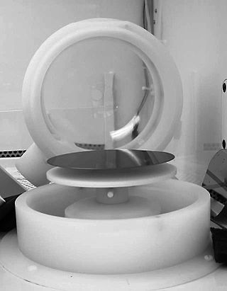
Spin coating is a procedure used to deposit uniform thin films onto flat substrates. Usually a small amount of coating material is applied on the center of the substrate, which is either spinning at low speed or not spinning at all. The substrate is then rotated at speeds up to 10,000 rpm to spread the coating material by centrifugal force. A machine used for spin coating is called a spin coater, or simply spinner.

In physics, a "coffee ring" is a pattern left by a puddle of particle-laden liquid after it evaporates. The phenomenon is named for the characteristic ring-like deposit along the perimeter of a spill of coffee. It is also commonly seen after spilling red wine. The mechanism behind the formation of these and similar rings is known as the coffee ring effect or in some instances, the coffee stain effect, or simply ring stain.
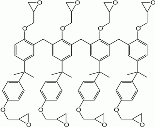
SU-8 is a commonly used epoxy-based negative photoresist. Negative refers to a photoresist whereby the parts exposed to UV become cross-linked, while the remainder of the film remains soluble and can be washed away during development.
Conformal coating is a protective, breathable coating of thin polymeric film applied to printed circuit boards (PCB). It is named as such because it conforms to the contours of the PCB. Conformal coatings are typically applied at 25–250 μm to the electronic circuitry and provide protection against moisture, dust, chemicals, and temperature extremities. More recently, conformal coatings have been used to reduce the formation of whiskers, and can also prevent current bleed between closely positioned components.
Nanofabrics are textiles engineered with small particles that give ordinary materials advantageous properties such as superhydrophobicity, odor and moisture elimination, increased elasticity and strength, and bacterial resistance. Depending on the desired property, a nanofabric is either constructed from nanoscopic fibers called nanofibers, or is formed by applying a solution containing nanoparticles to a regular fabric. Nanofabrics research is an interdisciplinary effort involving bioengineering, molecular chemistry, physics, electrical engineering, computer science, and systems engineering. Applications of nanofabrics have the potential to revolutionize textile manufacturing and areas of medicine such as drug delivery and tissue engineering.

Printed electronics is a set of printing methods used to create electrical devices on various substrates. Printing typically uses common printing equipment suitable for defining patterns on material, such as screen printing, flexography, gravure, offset lithography, and inkjet. By electronic-industry standards, these are low-cost processes. Electrically functional electronic or optical inks are deposited on the substrate, creating active or passive devices, such as thin film transistors; capacitors; coils; resistors. Some researchers expect printed electronics to facilitate widespread, very low-cost, low-performance electronics for applications such as flexible displays, smart labels, decorative and animated posters, and active clothing that do not require high performance.

Evaporation is a common method of thin-film deposition. The source material is evaporated in a vacuum. The vacuum allows vapor particles to travel directly to the target object (substrate), where they condense back to a solid state. Evaporation is used in microfabrication, and to make macro-scale products such as metallized plastic film.
Layer-by-layer (LbL) deposition is a thin film fabrication technique. The films are formed by depositing alternating layers of oppositely charged materials with wash steps in between. This can be accomplished by using various techniques such as immersion, spin, spray, electromagnetism, or fluidics.
Chemical Bath Deposition, also called Chemical Solution Deposition and CBD, is a method of thin-film deposition, using an aqueous precursor solution. Chemical Bath Deposition typically forms films using heterogeneous nucleation, to form homogeneous thin films of metal chalcogenides and many less common ionic compounds. Chemical Bath Deposition produces films reliably, using a simple process with little infrastructure, at low temperature (<100˚C), and at low cost. Furthermore, Chemical Bath Deposition can be employed for large-area batch processing or continuous deposition. Films produced by CBD are often used in semiconductors, photovoltaic cells, and supercapacitors, and there is increasing interest in using Chemical Bath Deposition to create nanomaterials.
Ceramic nanoparticle is a type of nanoparticle that is composed of ceramics, which are generally classified as inorganic, heat-resistant, nonmetallic solids that can be made of both metallic and nonmetallic compounds. The material offers unique properties. Macroscale ceramics are brittle and rigid and break upon impact. However, Ceramic nanoparticles take on a larger variety of functions, including dielectric, ferroelectric, piezoelectric, pyroelectric, ferromagnetic, magnetoresistive, superconductive and electro-optical.
Ion layer gas reaction (ILGAR®) is a non-vacuum, thin-film deposition technique developed and patented by the group of Professor Dr. Christian-Herbert Fischer at the Helmholtz-Zentrum Berlin for materials and energy in Berlin, Germany. It is a sequential and cyclic process that enables the deposition of semiconductor thin films, mainly for photovoltaic applications, specially chalcopyrite absorber layers and buffer layers. The ILGAR technique was awarded as German High Tech Champion 2011 by the Fraunhofer Society.
Nanosphere lithography (NSL) is an economical technique for generating single-layer hexagonally close packed or similar patterns of nanoscale features. Generally, NSL applies planar ordered arrays of nanometer-sized latex or silica spheres as lithography masks to fabricate nanoparticle arrays. NSL uses self-assembled monolayers of spheres as evaporation masks. These spheres can be deposited using multiple methods including Langmuir-Blodgett, Dip Coating, Spin Coating, solvent evaporation, force-assembly, and air-water interface. This method has been used to fabricate arrays of various nanopatterns, including gold nanodots with precisely controlled spacings.
Nanoparticle deposition refers to the process of attaching nanoparticles to solid surfaces called substrates to create coatings of nanoparticles. The coatings can have a monolayer or a multilayer and organized or unorganized structure based on the coating method used. Nanoparticles are typically difficult to deposit due to their physical properties.
Molecular layer deposition (MLD) is a vapour phase thin film deposition technique based on self-limiting surface reactions carried out in a sequential manner. Essentially, MLD resembles the well established technique of atomic layer deposition (ALD) but, whereas ALD is limited to exclusively inorganic coatings, the precursor chemistry in MLD can use small, bifunctional organic molecules as well. This enables, as well as the growth of organic layers in a process similar to polymerization, the linking of both types of building blocks together in a controlled way to build up organic-inorganic hybrid materials.

Slot-die coating is a coating technique for the application of solution, slurry, or extruded thin films onto typically flat substrates such as glass, metal, paper, fabric or plastic foils. The process was first developed for the industrial production of photographic papers in the 1950's. It has since become relevant in numerous commercial processes and nanomaterials related research fields.
