Electroless nickel coatings range from nickel boron and ternary alloys to highly functional composites. Nickel phosphorus deposits find the most use in the markets the plating industry serves.
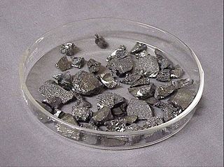
Boron is a chemical element with the symbol B and atomic number 5. Produced entirely by cosmic ray spallation and supernovae and not by stellar nucleosynthesis, it is a low-abundance element in the Solar system and in the Earth's crust. Boron is concentrated on Earth by the water-solubility of its more common naturally occurring compounds, the borate minerals. These are mined industrially as evaporites, such as borax and kernite. The largest known boron deposits are in Turkey, the largest producer of boron minerals.
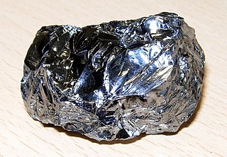
Phosphorus is a chemical element with the symbol P and atomic number 15. Elemental phosphorus exists in two major forms, white phosphorus and red phosphorus, but because it is highly reactive, phosphorus is never found as a free element on Earth. It has a concentration in the Earth's crust of about one gram per kilogram. With few exceptions, minerals containing phosphorus are in the maximally oxidized state as inorganic phosphate rocks.
Plating is a surface covering in which a metal is deposited on a conductive surface. Plating has been done for hundreds of years; it is also critical for modern technology. Plating is used to decorate objects, for corrosion inhibition, to improve solderability, to harden, to improve wearability, to reduce friction, to improve paint adhesion, to alter conductivity, to improve IR reflectivity, for radiation shielding, and for other purposes. Jewelry typically uses plating to give a silver or gold finish.
Electroless nickel (EN) deposits are typically classified as functional coatings and historically have found use in applications that require protection from either corrosion or wear and in some cases, both. Because of the unique deposit properties and uniformity of the resultant film, many other applications have emerged that continue to capitalize on the chameleon-like nature of electroless nickel. The majority of EN films used commercially are deposited from solutions formulated with sodium hypophosphite as the reducing agent.[1] This results in nickel films that are alloyed with phosphorus in ranges between 1 and 12 weight percent.
Corrosion is a natural process that converts a refined metal into a more chemically-stable form such as oxide, hydroxide, or sulfide. It is the gradual destruction of materials by chemical and/or electrochemical reaction with their environment. Corrosion engineering is the field dedicated to controlling and stopping corrosion.
Sodium hypophosphite (NaPO2H2, also known as sodium phosphinate) is the sodium salt of hypophosphorous acid and is often encountered as the monohydrate, NaPO2H2·H2O. It is a solid at room temperature, appearing as odorless white crystals. It is soluble in water, and easily absorbs moisture from the air.
The mechanical properties of NiP (ENP) deposits can be further enhanced not only by the co-deposition of inert particles such as teflon, silicon carbide or boron nitride but also by alloying with a third element, forming a ternary alloy of NiPX, where X can be copper, tungsten, molybdenum or tin depending on the particular formulation.
Silicon is a chemical element with the symbol Si and atomic number 14. It is a hard and brittle crystalline solid with a blue-grey metallic lustre; and it is a tetravalent metalloid and semiconductor. It is a member of group 14 in the periodic table: carbon is above it; and germanium, tin, and lead are below it. It is relatively unreactive. Because of its high chemical affinity for oxygen, it was not until 1823 that Jöns Jakob Berzelius was first able to prepare it and characterize it in pure form. Its melting and boiling points of 1414 °C and 3265 °C respectively are the second-highest among all the metalloids and nonmetals, being only surpassed by boron. Silicon is the eighth most common element in the universe by mass, but very rarely occurs as the pure element in the Earth's crust. It is most widely distributed in dusts, sands, planetoids, and planets as various forms of silicon dioxide (silica) or silicates. More than 90% of the Earth's crust is composed of silicate minerals, making silicon the second most abundant element in the Earth's crust after oxygen.
Boron nitride is a thermally and chemically resistant refractory compound of boron and nitrogen with the chemical formula BN. It exists in various crystalline forms that are isoelectronic to a similarly structured carbon lattice. The hexagonal form corresponding to graphite is the most stable and soft among BN polymorphs, and is therefore used as a lubricant and an additive to cosmetic products. The cubic variety analogous to diamond is called c-BN; it is softer than diamond, but its thermal and chemical stability is superior. The rare wurtzite BN modification is similar to lonsdaleite but slightly softer than the cubic form
Copper is a chemical element with the symbol Cu and atomic number 29. It is a soft, malleable, and ductile metal with very high thermal and electrical conductivity. A freshly exposed surface of pure copper has a pinkish-orange color. Copper is used as a conductor of heat and electricity, as a building material, and as a constituent of various metal alloys, such as sterling silver used in jewelry, cupronickel used to make marine hardware and coins, and constantan used in strain gauges and thermocouples for temperature measurement.
Electroless nickel boron (NiB) alloys are also well cited in the literature,[2] although they are less commercially viable than the NiP alloys. The films are generated using either sodium borohydride or dimethylaminoborane as the reducing agent and can range in boron content from 1–5 weight percent. NiB films are typically used in the electronics industry where low-resistivity coatings are required and also find use in industrial applications when extreme wear and increased coating hardness is specified.
Electroless nickel is no different than its electroplated counterparts in that it is only as strong as the weakest link in the process cycle. More clearly stated, successful electroless nickel plating requires both strict adherence to bath operating guidelines and optimal surface preparation. A well formulated electroless nickel process will not overcome improper surface preparation. Conversely, applying the wrong electroless nickel will short-circuit success even when the substrate is wonderfully prepared. The following links are critical:
Electroless nickel (EN) plating is an auto-catalytic reaction that deposits an even layer of nickel-phosphorus or nickel-boron alloy on the surface of a solid material, or substrate, like metal or plastic. The process involves dipping the substrate in a bath of plating solution, where a reducing agent, like hydrated sodium hypophosphite (NaPO2H2 · H2O), reacts with the material's ions to deposit the nickel alloy. The metallurgical properties of the alloy depend on the percentage of phosphorus, which can range from 2–5% (low phosphorus) to 11–14% (high phosphorus). Unlike electroplating, it is not necessary to pass an electric current through the plating solution to form a deposit. Electroless plating prevents corrosion and wear, and can be used to manufacture composite coatings by suspending powder in the bath. EN plating creates an even layer regardless of the geometry of the surface – in contrast to electroplating which suffers from flux-density issues as an electromagnetic field will vary due to the surface profile and result in uneven depositions. Depending on the catalyst, EN plating can be applied to non-conductive surfaces.
Proper surface preparation
Choice of electroless nickel
Conformance to operating guidelines.
Failing to recognize the interconnection between these three basic items will ultimately lead to failure of the plating, hopefully before the component reaches the field.
Physical and mechanical properties
Microstructure and composition of ENP Films
Figure 1Figure 2
One of the distinct advantages of the electroless nickel deposition process is the ability to produce an alloy of nickel and phosphorus in varying ratios. Depending on the formulation and the operation of the chemistry the film compositions can vary from 2 to 13 weight percent phosphorus.[3] This variation in alloy content has a significant effect on the deposit microstructure and performance characteristics and offers flexibility to well informed platers and engineers that can take full advantage of these differences.
Electrodeposited nickel has a purity of greater than 99% and is highly crystalline. On the other hand, electroless nickel deposits that contain more than 10.5% phosphorus appear to be amorphous, i.e., lacking crystal structure.[4] EN deposits with less than 7 weight percent phosphorus have a clear microcrystalline structure (2-6nm grain size) and film properties are distinctly different.[5] Some studies have found that higher phosphorus deposits (above 10.5 weight percent phosphorus) may not be truly amorphous but rather a mixture of microcrystalline and amorphous phases.
Deposits with a high degree of amorphous composition are free of grain boundaries, which typically act as sites for intergranular corrosion commonly encountered in crystalline deposits. There are also applications that benefit from crystalline structure as well. Duncan pointed out that in the as deposited condition an electroless nickel[6] coating can contain both crystalline and amorphous phases or, if dictated by formula, may only contain one phase. Each phase offers distinct benefits and understanding what exists in the deposit you plan to apply is relevant.[7]
Deposit uniformity
A significant advantage of the electroless nickel process is the ability to produce deposits with uniform thickness on parts with complex geometries and shapes.[8] Since this is a chemical reaction, any catalytic surface exposed to the plating solution will plate uniformly, provided it meets the criteria established a few paragraphs earlier. The current density effects typically associated with electroplating are not a factor, therefore sharp edges, deep recesses and blind holes are readily plated to uniform thickness with electroless nickel chemistry. Many applications for electroless nickel exist today because it is often the only way to plate certain components. The difference in deposit uniformity is illustrated in figure 1. Figure 2 is a photo of EN plated bumps on a flip chip, something impossible to accomplish with an electroplated deposit.
The degree of uniformity can vary on edges, threads, small holes or deep recesses where exchange of fresh solution may be difficult. This can also occur under conditions with excessive bath agitation, especially in the presence of heavy metals.[9] This thickness variation may be controlled by optimizing solution dynamics and/or by controlling the concentration of certain additives formulated into the EN plating bath.
Melting point
Figure 3
Unlike electroplated nickel, electroless nickel deposits do not have a precise melting point but rather have a melting range. Pure nickel has a melting point of 1455°C (2650°F), however EN is an alloy and as the phosphorus content is increased within the film, the deposit begins to soften at lower temperatures and continues to soften until it eventually melts. The melting range decreases linearly as the phosphorus levels increase. The eutectic or lowest melting point for NiP alloys is 880°C (1620°F) and occurs at a deposit phosphorus content of 11% b.w.[10] The highest melting point is for low Phosphorus deposits (less than 3%) that claim to have melting points at 1,200°C (2,200°F). EN has failed in some high temperature applications since it was not fully recognized that even with a relatively high melting range the deposit may still have a liquid phase at lower temperatures. Figure 3 illustrates what happens when you subject EN to temperatures above its melting point.
Electrical resistivity
The electrical resistivity of electroless nickel alloys is higher than that of pure nickel. High purity nickel has a specific resistivity of 7.8 x 10⁻⁶ ohm-cm. Increasing the phosphorus content increases the electrical resistivity of the film. (Figure 4.) Values range from 30-100 x 10-6 ohm-cm. Heat treatment of the ENP film can affect resistivity. At temperatures as low as 150°C resistivity will decrease due to release of physically adsorbed hydrogen. At temperatures greater than 250°C a similar marked decrease will occur as a result of phosphorus migration and the structural transformation to Nickel Phosphide.[11]
Figure 4
Magnetic properties
The single largest application for electroless nickel is as a sub layer for computer memory discs. To meet the requirements for this application the coating must remain non-magnetic even after one-hour bake cycles of 250-300°C. In recent years, the data storage industry has pushed the high side of this temperature range even higher. This can be achieved only with high phosphorus alloys (> 10.5% P) and/or with specific additives. The non-magnetic property of these high phosphorus films is one of the most important physical characteristics.[12] Figure 5 depicts the effect phosphorus content has on ferromagnetic properties.
Figure 5
Not all high phosphorus alloys will maintain the same level of thermomagnetic stability. The deposit performance is also dependent on the chemical formulation and the solution dynamics during the plating process. Reducing the onset and the rate of crystallization, minimizing the volume fraction of microcrystallinity and maintaining a homogeneous grain structure at higher bake temperatures are key requirements for optimization of the films thermomagnetic performance.[13]
The most widespread application of electroless nickel technology is to provide superior corrosion protection in a multitude of corrosive environments. Market data clearly indicates that the majority of applications for EN are on steel and aluminium substrates that are anodic or less noble than EN.[14] EN acts as a barrier coating that protects by providing a pore free barrier coating against the corrosive environment. This is in direct contrast to sacrificial films such as zinc or zinc alloy that protect the base material by sacrificing itself.
The nature of the corrosive environment and the deposit's resistance to chemical attack are also important criteria when selecting a particular EN coating for optimum performance. High phosphorus coatings (10-12%) are more readily attacked in strongly alkaline media than low phosphorus deposits (1-3%), however they perform significantly better in acidic media.[15] This is illustrated in the following graphs.
Optimizing the performance of EN coatings for maximum corrosion protection requires that the coating be continuous and free of any microporosity, roughness, nodules and irregularities within the microstructure. Since the microstructure of high phosphorus EN films are amorphous they are essentially free of the grain boundaries that could potentially serve as sites for corrosion. The absence of such phase boundaries and the ability of the high phosphorus EN film to form a passive film on its surface, make it an excellent choice for protection on aluminum and steel substrates in highly corrosive, acidic environments.[16]
The phosphorus content alone however is not enough to maximize the coatings corrosion resistance in a given environment. Factors that will affect the corrosion performance of EN films are:
1.Proper selection of the EN process and deposit thickness[17]
2.Operation and maintenance of the process, minimizing co-deposited impurities
3.Minimizing substrate defects through improved OEM training on substrate selection (cast vs extruded) and various pre-plate mechanical operations (forming, stamping, grinding, etc.)
4.Selecting the optimum pretreatment cycle
5.Post plate operations (both good and bad). Bad- High temperature post treatment that can produce micro-cracked deposits-Bad. Good-Post dips, low temperature bakes, etc.
Surface condition plays an important role in determining the required deposit thickness and good field performance. For example, machined substrates alloyed with sulfur and/or lead are particularly vulnerable to a high degree of porosity, since these alloying constituents are catalytic poisons to the deposition process. Substrates with high roughness values require thicker deposits to provide adequate corrosion protection. This is primarily due to the formation of nodules on the roughened surface during the initial stages of deposition, resulting in microporosity of the ENP film.
Increasing the deposit thickness can minimize this effect. Smooth substrates require a thickness of 25µm to obtain a film with minimal porosity whereas roughened surfaces can require up to three times the thickness to provide similar corrosion protection.[18]
The use of neutral salt spray, in accordance with the ASTM B 117 specification, for the measurement of corrosion performance is well documented in the literature and is still the most widely accepted method for coating evaluation.[19] The results of neutral salt spray exposure, phosphorus content and deposit thickness are summarized in the table below:
Corrosion Resistance per ASTM B-117 Neutral Salt Spray Test
Coating Thickness
4-5% ENP
7-8% ENP
6.5-8% ENP
10.5-12.0% ENP
12µm (0.4 mils)
24
24
24
250
22µm (0.8 mils)
96
96
96
1,000
38µm (1.4 mils)
96
96
96
1,000
50µm (2.0 mils)
96
96
96
1,000
Deposit hardness
Deposit hardness is one of the key tribological properties of ENP coating technology. Factors that affect hardness are the film composition (%P), the heat treatment temperature and the heat treatment time. Typical microhardness values for the as plated ENP deposits range from 500 to 720 VHN (Figure 8.) This is in contrast to electrolytically deposited nickel, which have typical values of 150-400VHN.[20]
Heat treatment of ENP deposit will significantly increase the microhardness. Figure 9 illustrates the effective temperature range and time required to attain specific values.
In cases where the substrate cannot withstand the temperature requirements to achieve maximum hardness, low phosphorus EN is often recommended. The increase in microhardness for ENP films is attributed to the phase transformations that take place during the heat cycle to form nickel metal and nickel phosphide. Some volume shrinkage and cracking of the film will occur and must be taken into account if the application requires corrosion protection.
Wear resistance
Electroless Nickel Phosphorus coatings are specified for a wide variety of engineered applications related to wear resistance. This is mainly attributed to the fact that the coatings not only have high hardness and intrinsic lubricity but also afford excellent corrosion resistance and deposit uniformity. The wear properties of ENP films can also be enhanced through the codeposition of inert particles such as PTFE, Silicon Carbide or Boron Nitride forming a composite coating.[18]
The abrasive wear of ENP films are typically measured by applying a mechanical action of an abrasive, rotating wheel on the plated surface and measuring the weight loss (in milligrams) of the coating at intervals of 1000 cycles. This test is referred to as the Taber Wear Index (TWI) and perhaps is the most frequently used method to evaluate the wear characteristics of ENP films.[21] Typical weight loss results for various deposits are illustrated in Figure 10.
The “as plated” low phosphorus deposits tend to withstand abrasive wear better than the high phosphorus coatings, largely attributed to the higher hardness values. However, after heat treatment the trends remain the same even though the deposit hardness is similar suggesting that other factors, such as deposit composition, play a role in abrasive wear resistance.
Adhesive wear is defined as the removal of material between mating surfaces and measures the films ability to resist galling, welding or seizing.[22] If the mating surfaces are both electroless nickel, optimum performance is achieved if the surfaces in contact have dissimilar properties, such as phosphorus content or hardness. The adhesive wear resistance of ENP films improves with increasing phosphorus content.[23]
It is important to consider as many variables as possible when evaluating an ENP coating for tribological applications. Factors such as hardness, phosphorus content, the presence of corrosive liquids or gases, the temperature, the nature of the mating surface, the degree of lubrication and the characteristics of the substrate are critical to optimum performance.
Lubricity
As pointed out above, lubricity plays an important role in optimizing wear resistance. It does so by inhibiting contact between mating surfaces, reducing friction and associated heat. Hard chrome is well known as possessing a self healing lubricating film. Whereas EN does not exhibit this feature it still offers excellent lubricity and finds many uses that can capitalize on this property.[24] Figure 11 graphically displays the coefficient of friction vs. non lubricated steel. Hard chrome does perform better than standard high phosphorus EN (HP EN) but with occlusion of various soft particles you can achieve much lower values.
Most wear environments have multiple points of contact and it is quite common that all mating surfaces are plated. The table below highlights the improved performance of electroless nickel when both mating surfaces are plated where the results are comparable to hard chrome.
Friction Coefficients of Several Mating Surfaces
Mating Surface
Coefficient of Friction
Unlubricated
Lubricated
Electroless nickel vs Steel
0.38
0.20
Chrome vs Steel
0.21
0.13
Steel vs Steel
galling
0.2
Chrome vs Chrome
0.43
0.26
EN vs EN
0.45
0.20
Electroless nickel vs Chrome
0.43
0.30
EN PTFE vs steel
0.12
EN Boron nitride vs steel
0.07
Ductility
Although electroless nickel is widely considered an engineering coating it does not compare well to other coatings in terms of certain mechanical properties. Ductility is one of these. Electroless nickel is considered a very strong yet brittle material. The relatively low ductility is due to the various microcrystalline and amorphous structures that limit plastic deformation,[25] i.e. the ability to “stretch” without fracture. It is not uncommon for heavy build deposits (in excess of 25µm) to crack when exposed to severe loads. This is especially evident in lower phosphorus films or those plated from older baths (in excess of 150g/l of orthophosphate) with high tensile stress.
Internal stress
Internal stress is arguably one of the most important mechanical properties of electroless nickel and often the most ignored. Internal stress plays a role in adhesion, wear and corrosion resistance and therefore must be regulated or at a minimum, taken notice of. Internal stress can be developed both extrinsically and intrinsically.
Extrinsic stress is the least insidious and is brought on by differences in thermal coefficient of expansion between the deposit and the substrate. When the plated surfaces are first cooled there is an inherent shrinkage of the component. Electroless nickel typically shrinks roughly 0.1% on cooling from the operating bath temperature. When plated on substrates that have a higher COTE than EN (brass and aluminum for example) the EN deposit will develop tensile stress. On substrates that have a lower COTE than EN the deposit will be in a compressive state. This of course, assumes no loss of adhesion or serious cracking as the component seeks to adjust to the shrinkage.
Intrinsic stress is brought on by the plating process itself. Although the substrate also plays a small role, intrinsic stress is controlled by formation of the nickel layers due primarily to the EN formulation and bath operating conditions. A general remark to guide your thought process would be that higher phosphorus EN processes operated under good practice will produce deposits with neutral or compressive stress. In most applications, compressive stress is desired since it has a negligible effect on fatigue loss, improves adhesion and some have found improved corrosion protection. The graph below in Figure 12 reflects deposit stress vs phosphorus content. Note that lower phosphorus deposits (less than 4% b.w.) will also exhibit lower tensile stress. This can attributed to the presence of homogeneous structural phases that Duncan reported years ago.[26]
Assuming the proper EN formulation is selected to deliver the desired stress level, a reduction in compressive stress or even a shift to tensile is possible under certain conditions and must be avoided. Operating an EN bath outside of its recommend guidelines will impact stress. As a plater desires to push a process to plate faster, raising the pH is often the first button to push. When the pH is increased the deposit phosphorus drops, compressive stress is reduced and this can lead to negative results.[27] Platers are commonly surprised to find a process that was plating with no stress cracks or adhesion failure the day before is now producing failures. A simple view of the record books or quick analysis reveals the culprit. An even more common contributor to an increase in an EN deposits tensile nature is bath age. It has been well documented that an EN process designed to produce a compressive deposit will stop doing so after a certain bath age (roughly 5 metal turnovers). It is at this point where the presence of reaction by products, sodium orthophosphate, begins to contribute to tensile stress. One can continue to plate in this bath but must be fully aware that stress will increase and could lead to adhesion and/or cracking failures. This is most evident, again, with thicker films. Figure 13 represents this phenomenon. There are certain additives that, when used carefully, can reduce the tensile stress even as the EN bath ages. The photos in figure 14 are of two identical parts, each plated in the same bath but at different bath ages. The part on the right was plated in a relatively new bath whereas the one on the left was plated in a bath nearly 10 metal turnovers old. You'll note the clear evidence of flaking and separation due to the high tensile stress.
Armed with a better understanding of the properties of electroless nickel phosphorus deposits, both platers and engineers alike should be able to effectively select the proper EN process as well as necessary operating guides for each and every application they encounter. The following section provides an overview of these applications.
Applications
Electroless nickel gained market acceptance over the past 50 years through a combination of trial and errors, excellent marketing initiatives and commitment from many plating shop pioneers willing to take on a fledgling technology. Today, electroless nickel offers the engineering community a technology that is as reliable as it is diverse in meeting various application challenges. An approximate breakdown of worldwide applications for electroless nickel is detailed below:
Automotive
Applications for use in this industry take full advantage of the many benefits electroless nickel has to offer. Deposit properties such as uniformity, corrosion resistance, lubricity and wear resistance are all reasons why the use of EN for automotive applications continues to grow. Historically, a cost sensitive market segment, auto makers have embraced the use low cost materials plated with a thin film of electroless nickel to meet strict requirements in an economical fashion. Fuel injection systems, aluminum fuel filters, brake pins and bleed valves are just a few applications that take full advantage of the deposit's corrosion resistance. Differential pinion shafts and a variety of pins and washers are plated in large quantities due to the coatings lubricity, wear resistance and anti-galling properties (Figure 15). Brake pistons are plated in bright, medium phosphorus electroless nickel and heat treated to increase hardness and wear resistance. High deposit luster is desired and actually improves the surface finish of the piston resulting in reduced friction (Figure 16). Cast iron slip yokes are plated with EN to eliminate noise associated with galling.
Future applications will most likely include the use of EN composites such as PTFE, boron nitride and silicon carbide. The use and growth of fuel cell technology in automobiles shows promise and electroless nickel could play a role. A challenge EN faced nearly a decade ago was the End-of Life Vehicle (ELV) directive[28] that bans the use of various toxic metals often found in EN deposits. Viewed as a barrier when it was first promulgated, many experts feel the ELV directive and other similar green initiatives have actually advanced EN technology.
Aerospace
Design engineers have found the combination of electroless nickel's functional properties to be very appealing for aerospace use. Due to the obvious reliability issues associated with this market segment, a long term, thorough evaluation of electroless nickel has been on going and had made for slow progress. Successful testing and application for a number of years resulted in a better understanding of when and how to specify electroless nickel. It is widely used in engine assemblies, servo valves, landing gear, turbine blades and the like. Unlike hard chrome, compressive stressed high phosphorus deposits do not significantly reduce the fatigue strength of these critical components. For this reason and reasons stated above, its continued application appears secure.[citation needed]
Electronics
Use of electroless nickel for electronic applications continues to grow and is clearly the most diverse market segment. Magnetic properties, corrosion resistance and solderability are properties that have contributed the most to its success. A large application involves the use of high phosphorus deposits on polished aluminium substrates for magnetic data storage on computers. Uniformity, non-magnetic character and reliably smooth, defect free nature lend to its continued use. Over the past 20 years this application for EN has been threatened a number of times by emerging technology. In each case, EN has proven up to the challenge and maintained its position as the most reliable and cost effective technology. (Figure 17)
Heat sinks, semiconductor packages, and battery components are examples of other high volume electroless nickel electronic applications (Figure 18). A variety of aluminium and zinc die cast connectors are plated with EN to enhance corrosion and wear resistance (Figure 19). Uniformity, electrical conductivity and solderability are other important properties for this application.
An area of continued interest and growth is the plating of microwave components. With complex shapes and deep recessed areas electroless nickel is ideally suited to act as a corrosion resistant barrier film on top of aluminum and beneath the silver or tin electroplated topcoat.
Although certain technical barriers must be overcome, the use of medium phosphorus electroless nickel beneath immersion gold on circuit boards, shows promise. Commonly referred to as the ENIG (Electroless nickel immersion gold) process, it offers improved shelf life in humid conditions and maintains excellent solderability over periods of long storage.
Renewable energy also appears to offer promise for EN where its use for metalizing photovoltaic cells is developing quickly.
Chemical processing
Requirements for this application often include the need to maintain product purity in addition to the typical needs for uniformity and corrosion resistance. Selecting the proper electroless nickel is often critical to successful application. Recent studies have found phosphorus content plays an important role in the overall performance of the EN deposit in a specific environment. Pumps, valves and flanges are typically plated with 50-100µm of electroless nickel for very severe applications.
Oil and gas industry
A proving ground for electroless nickel over the past 25 years, the success of electroless nickel for these applications is well documented. Ball valves, heat exchangers, pumps, etc. fabricated from less expensive materials and plated with high phosphorus EN has greatly contributed to the success. Corrosion resistance in harsh environments and resistance to erosive wear as well as its uniformity will allow EN to maintain its dominant position in this market segment.
Other applications
Food handling, mold protection, foundry tooling, plating on non-conductors and the printing industry are a few other applications where electroless nickel finds significant use. Textile applications (Figure 20) utilize excellent wear resistance and lubricity characteristics. Composite coatings such as EN/boron nitride have found increased use in applications that require extending service life (Figure 21).
The following is a table that offers a general guide to selecting an electroless nickel for a specific application or requirement:
Electroplating is a process that uses an electric current to reduce dissolved metal cations so that they form a thin coherent metal coating on an electrode. The term is also used for electrical oxidation of anions on to a solid substrate, as in the formation of silver chloride on silver wire to make silver/silver-chloride electrodes. Electroplating is primarily used to change the surface properties of an object, but may also be used to build up thickness on undersized parts or to form objects by electroforming.
Cupronickel or copper-nickel (CuNi) is an alloy of copper that contains nickel and strengthening elements, such as iron and manganese. The copper content typically varies from 60 to 90 percent.
Chrome plating, often referred to simply as chrome, is a technique of electroplating a thin layer of chromium onto a metal object. The chromed layer can be decorative, provide corrosion resistance, ease cleaning procedures, or increase surface hardness. Sometimes, a less expensive imitator of chrome may be used for aesthetic purposes.
Anodising is an electrolytic passivation process used to increase the thickness of the natural oxide layer on the surface of metal parts.
Copper plating is the process of plating a layer of copper electrolytically on the surface of an item. It takes place in an electrolytic cell where electrolysis which uses direct electric current to dissolve a copper rod and transport the copper ions to the item. Into a container of water are placed a copper rod, and the item. The water contains an ionic solution which allows a direct electric current to flow from the copper rod to the item. The copper rod is the anode and the item is the cathode. This current flow causes the copper to ionize, become oxidized which means each atom becomes positively charged by losing an electron. As the copper ions dissolve into the water, they form a coordination complex with salts already present. The copper then physically flows to the item, where it is reduced to the metallic state by gaining electrons. This forms a thin, solid, metallic copper film on the surface of the item.
Gold plating is a method of depositing a thin layer of gold onto the surface of another metal, most often copper or silver, by chemical or electrochemical plating. This article covers plating methods used in the modern electronics industry; for more traditional methods, often used for much larger objects, see gilding.
Metallizing is the general name for the technique of coating metal on the surface of objects. Metallic coatings may be decorative, protective or functional.
A coating is a covering that is applied to the surface of an object, usually referred to as the substrate. The purpose of applying the coating may be decorative, functional, or both. The coating itself may be an all-over coating, completely covering the substrate, or it may only cover parts of the substrate. An example of all of these types of coating is a product label on many drinks bottles- one side has an all-over functional coating and the other side has one or more decorative coatings in an appropriate pattern to form the words and images.
Super black is a surface treatment developed at the National Physical Laboratory (NPL) in the United Kingdom. It absorbs approximately 99.6% of visible light at normal incidence, while conventional black paint absorbs about 97.5%. At other angles of incidence, super black is even more effective: at an angle of 45°, it absorbs 99.9% of light.
Plasma electrolytic oxidation (PEO), also known as electrolytic plasma oxidation (EPO) or microarc oxidation (MAO), is an electrochemical surface treatment process for generating oxide coatings on metals. It is similar to anodizing, but it employs higher potentials, so that discharges occur and the resulting plasma modifies the structure of the oxide layer. This process can be used to grow thick, largely crystalline, oxide coatings on metals such as aluminium, magnesium and titanium. Because they can present high hardness and a continuous barrier, these coatings can offer protection against wear, corrosion or heat as well as electrical insulation.
Substrate is a term used in materials science to describe the base material on which processing is conducted to produce new film or layers of material such as deposited coatings.
Electroless nickel immersion gold (ENIG) is a type of surface plating used for printed circuit boards. It consists of an electroless nickel plating covered with a thin layer of immersion gold, which protects the nickel from oxidation.
AlBeMet is the trade name for a beryllium and aluminium metal matrix composite material derived by a powder metallurgy process. AlBeMet AM162 is manufactured by Materion Corporation Brush Beryllium and Composites.
Anti-corrosion refers to the protection of metal surfaces from corroding in high-risk (corrosive) environments.
Zinc alloy electroplating is an electrogalvanization process for corrosion protection of metal surfaces and increasing their wear resistance.
Nickel electroplating is a technique of electroplating a thin layer of nickel onto a metal object. The nickel layer can be decorative, provide corrosion resistance, wear resistance, or used to build up worn or undersized parts for salvage purposes.
Alkaline electroless nickel boron coating (NiB) is an autocatalytic coating process. The coating is deposited from an aqueous solution which contains either an alkylamineborane or sodium borohydride as a reducing agent, a source of nickel ions, a buffer, complexant, and control chemicals. Alkaline nickel boron coatings are classified as Type 1, Nickel thallium boron or Type 2, nickel boron.
↑ Ashassi-Sorkhabi, H.; Rafizadeh, S.H. (2004). "Effect of coating time and heat treatment on structures and corrosion characteristics of electroless Ni–P alloy deposits". Surface and Coatings Technology. 176 (3): 318–326. doi:10.1016/S0257-8972(03)00746-1.
↑ Chen, Yung-I; Duh, Jenq-Gong (1991). "TiN coatings on mild steel substrates with electroless nickel as an interlayer". Surface and Coatings Technology. 48 (2): 163–168. doi:10.1016/0257-8972(91)90140-R.
↑ Jean LaPlante (2005). "Building a platform for growth: Technology advances in electroless nickel provide practical benefits for platers". Metal Finishing. 103 (12): 18–24. doi:10.1016/S0026-0576(05)80844-X.
This page is based on this Wikipedia article Text is available under the CC BY-SA 4.0 license; additional terms may apply. Images, videos and audio are available under their respective licenses.