Related Research Articles
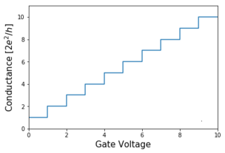
The quantum Hall effect is a quantized version of the Hall effect which is observed in two-dimensional electron systems subjected to low temperatures and strong magnetic fields, in which the Hall resistance Rxy exhibits steps that take on the quantized values
Spintronics, also known as spin electronics, is the study of the intrinsic spin of the electron and its associated magnetic moment, in addition to its fundamental electronic charge, in solid-state devices. The field of spintronics concerns spin-charge coupling in metallic systems; the analogous effects in insulators fall into the field of multiferroics.
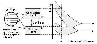
In solid-state physics and solid-state chemistry, a band gap, also called a bandgap or energy gap, is an energy range in a solid where no electronic states exist. In graphs of the electronic band structure of solids, the band gap refers to the energy difference between the top of the valence band and the bottom of the conduction band in insulators and semiconductors. It is the energy required to promote an electron from the valence band to the conduction band. The resulting conduction-band electron are free to move within the crystal lattice and serve as charge carriers to conduct electric current. It is closely related to the HOMO/LUMO gap in chemistry. If the valence band is completely full and the conduction band is completely empty, then electrons cannot move within the solid because there are no available states. If the electrons are not free to move within the crystal lattice, then there is no generated current due to no net charge carrier mobility. However, if some electrons transfer from the valence band to the conduction band, then current can flow. Therefore, the band gap is a major factor determining the electrical conductivity of a solid. Substances having large band gaps are generally insulators, those with small band gaps are semiconductor, and conductors either have very small band gaps or none, because the valence and conduction bands overlap to form a continuous band.
A heterojunction is an interface between two layers or regions of dissimilar semiconductors. These semiconducting materials have unequal band gaps as opposed to a homojunction. It is often advantageous to engineer the electronic energy bands in many solid-state device applications, including semiconductor lasers, solar cells and transistors. The combination of multiple heterojunctions together in a device is called a heterostructure, although the two terms are commonly used interchangeably. The requirement that each material be a semiconductor with unequal band gaps is somewhat loose, especially on small length scales, where electronic properties depend on spatial properties. A more modern definition of heterojunction is the interface between any two solid-state materials, including crystalline and amorphous structures of metallic, insulating, fast ion conductor and semiconducting materials.

A polaron is a quasiparticle used in condensed matter physics to understand the interactions between electrons and atoms in a solid material. The polaron concept was proposed by Lev Landau in 1933 and Solomon Pekar in 1946 to describe an electron moving in a dielectric crystal where the atoms displace from their equilibrium positions to effectively screen the charge of an electron, known as a phonon cloud. This lowers the electron mobility and increases the electron's effective mass.
A two-dimensional electron gas (2DEG) is a scientific model in solid-state physics. It is an electron gas that is free to move in two dimensions, but tightly confined in the third. This tight confinement leads to quantized energy levels for motion in the third direction, which can then be ignored for most problems. Thus the electrons appear to be a 2D sheet embedded in a 3D world. The analogous construct of holes is called a two-dimensional hole gas (2DHG), and such systems have many useful and interesting properties.
A Wigner crystal is the solid (crystalline) phase of electrons first predicted by Eugene Wigner in 1934. A gas of electrons moving in a uniform, inert, neutralizing background will crystallize and form a lattice if the electron density is less than a critical value. This is because the potential energy dominates the kinetic energy at low densities, so the detailed spatial arrangement of the electrons becomes important. To minimize the potential energy, the electrons form a bcc lattice in 3D, a triangular lattice in 2D and an evenly spaced lattice in 1D. Most experimentally observed Wigner clusters exist due to the presence of the external confinement, i.e. external potential trap. As a consequence, deviations from the b.c.c or triangular lattice are observed. A crystalline state of the 2D electron gas can also be realized by applying a sufficiently strong magnetic field. However, it is still not clear whether it is the Wigner crystallization that has led to observation of insulating behaviour in magnetotransport measurements on 2D electron systems, since other candidates are present, such as Anderson localization.
A quantum point contact (QPC) is a narrow constriction between two wide electrically conducting regions, of a width comparable to the electronic wavelength.
First introduced by M. Pollak, the Coulomb gap is a soft gap in the single-particle density of states (DOS) of a system of interacting localized electrons. Due to the long-range Coulomb interactions, the single-particle DOS vanishes at the chemical potential, at low enough temperatures, such that thermal excitations do not wash out the gap.

A topological insulator is a material whose interior behaves as an electrical insulator while its surface behaves as an electrical conductor, meaning that electrons can only move along the surface of the material.
A trion is a bound state of three charged particles. A negatively charged trion in crystals consists of two electrons and one hole, while a positively charged trion consists of two holes and one electron. The binding energy of a trion is largely determined by the exchange interaction between the two electrons (holes). The ground state of a negatively charged trion is a singlet. The triplet state is unbound in the absence of an additional potential or sufficiently strong magnetic field.
Silicene is a two-dimensional allotrope of silicon, with a hexagonal honeycomb structure similar to that of graphene. Contrary to graphene, silicene is not flat, but has a periodically buckled topology; the coupling between layers in silicene is much stronger than in multilayered graphene; and the oxidized form of silicene, 2D silica, has a very different chemical structure from graphene oxide.
Valleytronics is an experimental area in semiconductors that exploits local extrema ("valleys") in the electronic band structure. Certain semiconductors have multiple "valleys" in the electronic band structure of the first Brillouin zone, and are known as multivalley semiconductors. Valleytronics is the technology of control over the valley degree of freedom, a local maximum/minimum on the valence/conduction band, of such multivalley semiconductors.
James P. Eisenstein is an American physicist noted for his experimental research on strongly interacting two-dimensional electron systems. He is currently the Frank J. Roshek Professor of Physics and Applied Physics, Emeritus, at the California Institute of Technology.
Kenneth John Button was a solid-state and plasma physicist. He was the editor-in-chief of the International Journal of Infrared and Millimeter Waves from its inception in 1980 until his resignation in 2004.
Graphene is a semimetal whose conduction and valence bands meet at the Dirac points, which are six locations in momentum space, the vertices of its hexagonal Brillouin zone, divided into two non-equivalent sets of three points. The two sets are labeled K and K′. The sets give graphene a valley degeneracy of gv = 2. By contrast, for traditional semiconductors the primary point of interest is generally Γ, where momentum is zero. Four electronic properties separate it from other condensed matter systems.

Twistronics is the study of how the angle between layers of two-dimensional materials can change their electrical properties. Materials such as bilayer graphene have been shown to have vastly different electronic behavior, ranging from non-conductive to superconductive, that depends sensitively on the angle between the layers. The term was first introduced by the research group of Efthimios Kaxiras at Harvard University in their theoretical treatment of graphene superlattices.

An electron-on-helium qubit is a quantum bit for which the orthonormal basis states |0⟩ and |1⟩ are defined by quantized motional states or alternatively the spin states of an electron trapped above the surface of liquid helium. The electron-on-helium qubit was proposed as the basic element for building quantum computers with electrons on helium by Platzman and Dykman in 1999.
Aron Pinczuk was an Argentine-American experimental condensed matter physicist who was professor of physics and professor of applied physics at Columbia University. He was known for his work on correlated electronic states in two dimensional systems using photoluminescence and resonant inelastic light scattering methods. He was a fellow of the American Physical Society, the American Association for the Advancement of Science and the American Academy of Arts and Sciences.
Alan Harold Luther is an American physicist, specializing in condensed matter physics.
References
- ↑ "Frank F. Fang. Biography". Physics History Network. AIP.
- ↑ Fowler, AB; Fang, FF; Howard, WE; Stiles PJ (16 May 1966). "Magneto-Oscillatory Conductance in Silicon Surfaces". Physical Review Letters. 16 (20): 901–903. Bibcode:1966PhRvL..16..901F. doi:10.1103/PhysRevLett.16.901.
- ↑ IEEE Fellows Directory (Citation: For discovery and understanding of the two-dimensional properties of silicon inversion layers and for contributions to semiconductor device physics research.)
- ↑ Stern, Frank; Howard, WE (15 November 1967). "Properties of Semiconductor Surface Inversion Layers in the Electric Quantum Limit". Physical Review. 163 (3): 816–835. Bibcode:1967PhRv..163..816S. doi:10.1103/PhysRev.163.816.
| | This article about an American physicist is a stub. You can help Wikipedia by expanding it. |