
In electronic engineering, ground bounce is a phenomenon associated with transistor switching where the gate voltage can appear to be less than the local ground potential, causing the unstable operation of a logic gate.
In electronic engineering, ground bounce is a phenomenon associated with transistor switching where the gate voltage can appear to be less than the local ground potential, causing the unstable operation of a logic gate.
Ground bounce is usually seen on high density VLSI where insufficient precautions have been taken to supply a logic gate with a sufficiently low impedance connection to ground (or sufficiently high bypass capacitance). In this phenomenon, when the base of an NPN transistor is turned on, enough current flows through the emitter-collector circuit that the silicon in the immediate vicinity of the emitter-ground connection is pulled partially high, sometimes by several volts, thus raising the local ground, as perceived at the gate, to a value significantly above true ground. Relative to this local ground, the base voltage can go negative, thus shutting off the transistor. As the excess local charge dissipates, the transistor turns back on, possibly causing a repeat of the phenomenon, sometimes up to a half-dozen bounces.
Ground bounce is one of the leading causes of "hung" or metastable gates in modern digital circuit design. This happens because the ground bounce puts the input of a flip flop effectively at voltage level that is neither a one nor a zero at clock time, or causes untoward effects in the clock itself. A similar voltage sag phenomenon may be seen on the collector side, called supply voltage sag (or VCC sag), where VCC is pulled unnaturally low. As a whole, ground bounce is a major issue in nanometer range technologies in VLSI.
Ground bounce can also occur when the circuit board has poorly designed ground paths. Improper ground or VCC can lead to local variations in the ground level between various components. This is most commonly seen in circuit boards that have ground and VCC paths on the surfaces of the board.
Ground bounce may be reduced by placing a 10–30-ohm resistor in series to each of the switching outputs to limit the current flow during the gate switch. [1]

A multivibrator is an electronic circuit used to implement a variety of simple two-state devices such as relaxation oscillators, timers, latches and flip-flops. The first multivibrator circuit, the astable multivibrator oscillator, was invented by Henri Abraham and Eugene Bloch during World War I. It consisted of two vacuum tube amplifiers cross-coupled by a resistor-capacitor network. They called their circuit a "multivibrator" because its output waveform was rich in harmonics. A variety of active devices can be used to implement multivibrators that produce similar harmonic-rich wave forms; these include transistors, neon lamps, tunnel diodes and others. Although cross-coupled devices are a common form, single-element multivibrator oscillators are also common.
Transistor–transistor logic (TTL) is a logic family built from bipolar junction transistors. Its name signifies that transistors perform both the logic function and the amplifying function, as opposed to earlier resistor–transistor logic (RTL) and diode–transistor logic (DTL).

A bipolar junction transistor (BJT) is a type of transistor that uses both electrons and electron holes as charge carriers. In contrast, a unipolar transistor, such as a field-effect transistor (FET), uses only one kind of charge carrier. A bipolar transistor allows a small current injected at one of its terminals to control a much larger current flowing between the terminals, making the device capable of amplification or switching.

Complementary metal–oxide–semiconductor is a type of metal–oxide–semiconductor field-effect transistor (MOSFET) fabrication process that uses complementary and symmetrical pairs of p-type and n-type MOSFETs for logic functions. CMOS technology is used for constructing integrated circuit (IC) chips, including microprocessors, microcontrollers, memory chips, and other digital logic circuits. CMOS technology is also used for analog circuits such as image sensors, data converters, RF circuits, and highly integrated transceivers for many types of communication.
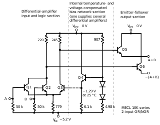
In electronics, emitter-coupled logic (ECL) is a high-speed integrated circuit bipolar transistor logic family. ECL uses an overdriven bipolar junction transistor (BJT) differential amplifier with single-ended input and limited emitter current to avoid the saturated region of operation and its slow turn-off behavior. As the current is steered between two legs of an emitter-coupled pair, ECL is sometimes called current-steering logic (CSL), current-mode logic (CML) or current-switch emitter-follower (CSEF) logic.

In electronics, a Schmitt trigger is a comparator circuit with hysteresis implemented by applying positive feedback to the noninverting input of a comparator or differential amplifier. It is an active circuit which converts an analog input signal to a digital output signal. The circuit is named a trigger because the output retains its value until the input changes sufficiently to trigger a change. In the non-inverting configuration, when the input is higher than a chosen threshold, the output is high. When the input is below a different (lower) chosen threshold the output is low, and when the input is between the two levels the output retains its value. This dual threshold action is called hysteresis and implies that the Schmitt trigger possesses memory and can act as a bistable multivibrator. There is a close relation between the two kinds of circuits: a Schmitt trigger can be converted into a latch and a latch can be converted into a Schmitt trigger.
Resistor–transistor logic (RTL), sometimes also known as transistor–resistor logic (TRL), is a class of digital circuits built using resistors as the input network and bipolar junction transistors (BJTs) as switching devices. RTL is the earliest class of transistorized digital logic circuit; it was succeeded by diode–transistor logic (DTL) and transistor–transistor logic (TTL).

Diode–transistor logic (DTL) is a class of digital circuits that is the direct ancestor of transistor–transistor logic. It is called so because the logic gating functions AND and OR are performed by diode logic, while logical inversion (NOT) and amplification is performed by a transistor.
In Boolean algebra, any Boolean function can be expressed in the canonical disjunctive normal form (CDNF), minterm canonical form, or Sum of Products as a disjunction (OR) of minterms. The De Morgan dual is the canonical conjunctive normal form (CCNF), maxterm canonical form, or Product of Sums which is a conjunction (AND) of maxterms. These forms can be useful for the simplification of Boolean functions, which is of great importance in the optimization of Boolean formulas in general and digital circuits in particular.
In computer engineering, a logic family is one of two related concepts:

IC power-supply pins denote a voltage and current supply terminals in electric, electronics engineering, and in integrated circuit design. Integrated circuits (ICs) have at least two pins that connect to the power rails of the circuit in which they are installed. These are known as the power-supply pins. However, the labeling of the pins varies by IC family and manufacturer. The double subscript notation usually corresponds to a first letter in a given IC family (transistors) notation of the terminals.

In electronic logic circuits, a pull-up resistor (PU) or pull-down resistor (PD) is a resistor used to ensure a known state for a signal. It is typically used in combination with components such as switches and transistors, which physically interrupt the connection of subsequent components to ground or to VCC. Closing the switch creates a direct connection to ground or VCC, but when the switch is open, the rest of the circuit would be left floating.

In electronics, metastability is the ability of a digital electronic system to persist for an unbounded time in an unstable equilibrium or metastable state. In digital logic circuits, a digital signal is required to be within certain voltage or current limits to represent a '0' or '1' logic level for correct circuit operation; if the signal is within a forbidden intermediate range it may cause faulty behavior in logic gates the signal is applied to. In metastable states, the circuit may be unable to settle into a stable '0' or '1' logic level within the time required for proper circuit operation. As a result, the circuit can act in unpredictable ways, and may lead to a system failure, sometimes referred to as a "glitch". Metastability is an instance of the Buridan's ass paradox.

Integrated injection logic (IIL, I2L, or I2L) is a class of digital circuits built with multiple collector bipolar junction transistors (BJT). When introduced it had speed comparable to TTL yet was almost as low power as CMOS, making it ideal for use in VLSI (and larger) integrated circuits. The gates can be made smaller with this logic family than with CMOS because complementary transistors are not needed. Although the logic voltage levels are very close (High: 0.7V, Low: 0.2V), I2L has high noise immunity because it operates by current instead of voltage. I2L was developed in 1971 by Siegfried K. Wiedmann and Horst H. Berger who originally called it merged-transistor logic (MTL). A disadvantage of this logic family is that the gates draw power when not switching unlike with CMOS.
Open collector, open drain, open emitter, and open source refer to integrated circuit (IC) output pin configurations that process the IC's internal function through a transistor with an exposed terminal that is internally unconnected. One of the IC's internal high or low voltage rails typically connects to another terminal of that transistor. When the transistor is off, the output is internally disconnected from any internal power rail, a state called "high-impedance" (Hi-Z). Open outputs configurations thus differ from push–pull outputs, which use a pair of transistors to output a specific voltage or current.
In integrated circuit design, dynamic logic is a design methodology in combinational logic circuits, particularly those implemented in metal–oxide–semiconductor (MOS) technology. It is distinguished from the so-called static logic by exploiting temporary storage of information in stray and gate capacitances. It was popular in the 1970s and has seen a recent resurgence in the design of high-speed digital electronics, particularly central processing units (CPUs). Dynamic logic circuits are usually faster than static counterparts and require less surface area, but are more difficult to design. Dynamic logic has a higher average rate of voltage transitions than static logic, but the capacitive loads being transitioned are smaller so the overall power consumption of dynamic logic may be higher or lower depending on various tradeoffs. When referring to a particular logic family, the dynamic adjective usually suffices to distinguish the design methodology, e.g. dynamic CMOS or dynamic SOI design.

Domino logic is a CMOS-based evolution of dynamic logic techniques consisting of a dynamic logic gate cascaded into a static CMOS inverter. The term derives from the fact that in domino logic, each stage ripples the next stage for evaluation, similar to dominoes falling one after the other. Domino logic contrasts with other solutions to the cascade problem where cascading is interrupted by clocks or other means.

Direct-coupled transistor logic (DCTL) is similar to resistor–transistor logic (RTL) but the input transistor bases are connected directly to the collector outputs without any base resistors. Consequently, DCTL gates have fewer components, are more economical, and are simpler to fabricate onto integrated circuits than RTL gates. Unfortunately, DCTL has much smaller signal levels, has more susceptibility to ground noise, and requires matched transistor characteristics. The transistors are also heavily overdriven; that is a good feature in that it reduces the saturation voltage of the output transistors, but it also slows the circuit down due to a high stored charge in the base. Gate fan-out is limited due to "current hogging": if the transistor base-emitter voltages are not well matched, then the base-emitter junction of one transistor may conduct most of the input drive current at such a low base-emitter voltage that other input transistors fail to turn on.
In electronics, pass transistor logic (PTL) describes several logic families used in the design of integrated circuits. It reduces the count of transistors used to make different logic gates, by eliminating redundant transistors. Transistors are used as switches to pass logic levels between nodes of a circuit, instead of as switches connected directly to supply voltages. This reduces the number of active devices, but has the disadvantage that the difference of the voltage between high and low logic levels decreases at each stage. Each transistor in series is less saturated at its output than at its input. If several devices are chained in series in a logic path, a conventionally constructed gate may be required to restore the signal voltage to the full value. By contrast, conventional CMOS logic switches transistors so the output connects to one of the power supply rails, so logic voltage levels in a sequential chain do not decrease. Simulation of circuits may be required to ensure adequate performance.
A gate driver is a power amplifier that accepts a low-power input from a controller IC and produces a high-current drive input for the gate of a high-power transistor such as an IGBT or power MOSFET. Gate drivers can be provided either on-chip or as a discrete module. In essence, a gate driver consists of a level shifter in combination with an amplifier. A gate driver IC serves as the interface between control signals and power switches. An integrated gate-driver solution reduces design complexity, development time, bill of materials (BOM), and board space while improving reliability over discretely-implemented gate-drive solutions.