Related Research Articles

Chemical vapor deposition (CVD) is a vacuum deposition method used to produce high quality, and high-performance, solid materials. The process is often used in the semiconductor industry to produce thin films.

Microelectromechanical systems (MEMS), also written as micro-electro-mechanical systems and the related micromechatronics and microsystems constitute the technology of microscopic devices, particularly those with moving parts. They merge at the nanoscale into nanoelectromechanical systems (NEMS) and nanotechnology. MEMS are also referred to as micromachines in Japan and microsystem technology (MST) in Europe.
In integrated circuit manufacturing, photolithography or optical lithography is a general term used for techniques that use light to produce minutely patterned thin films of suitable materials over a substrate, such as a silicon wafer, to protect selected areas of it during subsequent etching, deposition, or implantation operations. Typically, ultraviolet light is used to transfer a geometric design from an optical mask to a light-sensitive chemical (photoresist) coated on the substrate. The photoresist either breaks down or hardens where it is exposed to light. The patterned film is then created by removing the softer parts of the coating with appropriate solvents.
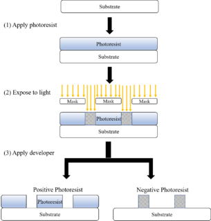
A photoresist is a light-sensitive material used in several processes, such as photolithography and photoengraving, to form a patterned coating on a surface. This process is crucial in the electronic industry.
In semiconductor technology, copper interconnects are interconnects made of copper. They are used in silicon integrated circuits (ICs) to reduce propagation delays and power consumption. Since copper is a better conductor than aluminium, ICs using copper for their interconnects can have interconnects with narrower dimensions, and use less energy to pass electricity through them. Together, these effects lead to ICs with better performance. They were first introduced by IBM, with assistance from Motorola, in 1997.
In semiconductor manufacturing, a low-κ is a material with a small relative dielectric constant relative to silicon dioxide. Low-κ dielectric material implementation is one of several strategies used to allow continued scaling of microelectronic devices, colloquially referred to as extending Moore's law. In digital circuits, insulating dielectrics separate the conducting parts from one another. As components have scaled and transistors have gotten closer together, the insulating dielectrics have thinned to the point where charge build up and crosstalk adversely affect the performance of the device. Replacing the silicon dioxide with a low-κ dielectric of the same thickness reduces parasitic capacitance, enabling faster switching speeds and lower heat dissipation. In conversation such materials may be referred to as "low-k" rather than "low-κ" (low-kappa).
Dry etching refers to the removal of material, typically a masked pattern of semiconductor material, by exposing the material to a bombardment of ions that dislodge portions of the material from the exposed surface. A common type of dry etching is reactive-ion etching. Unlike with many of the wet chemical etchants used in wet etching, the dry etching process typically etches directionally or anisotropically.
Chemical mechanical polishing (CMP) or planarization is a process of smoothing surfaces with the combination of chemical and mechanical forces. It can be thought of as a hybrid of chemical etching and free abrasive polishing.
In semiconductor fabrication, a resist is a thin layer used to transfer a circuit pattern to the semiconductor substrate which it is deposited upon. A resist can be patterned via lithography to form a (sub)micrometer-scale, temporary mask that protects selected areas of the underlying substrate during subsequent processing steps. The material used to prepare said thin layer is typically a viscous solution. Resists are generally proprietary mixtures of a polymer or its precursor and other small molecules that have been specially formulated for a given lithography technology. Resists used during photolithography are called photoresists.
Deep reactive-ion etching (DRIE) is a highly anisotropic etch process used to create deep penetration, steep-sided holes and trenches in wafers/substrates, typically with high aspect ratios. It was developed for microelectromechanical systems (MEMS), which require these features, but is also used to excavate trenches for high-density capacitors for DRAM and more recently for creating through silicon vias (TSVs) in advanced 3D wafer level packaging technology. In DRIE, the substrate is placed inside a reactor, and several gases are introduced. A plasma is struck in the gas mixture which breaks the gas molecules into ions. The ions accelerated towards, and react with the surface of the material being etched, forming another gaseous element. This is known as the chemical part of the reactive ion etching. There is also a physical part, if ions have enough energy, they can knock atoms out of the material to be etched without chemical reaction.
Nanoimprint lithography (NIL) is a method of fabricating nanometer scale patterns. It is a simple nanolithography process with low cost, high throughput and high resolution. It creates patterns by mechanical deformation of imprint resist and subsequent processes. The imprint resist is typically a monomer or polymer formulation that is cured by heat or UV light during the imprinting. Adhesion between the resist and the template is controlled to allow proper release.
Plasma etching is a form of plasma processing used to fabricate integrated circuits. It involves a high-speed stream of glow discharge (plasma) of an appropriate gas mixture being shot at a sample. The plasma source, known as etch species, can be either charged (ions) or neutral. During the process, the plasma generates volatile etch products at room temperature from the chemical reactions between the elements of the material etched and the reactive species generated by the plasma. Eventually the atoms of the shot element embed themselves at or just below the surface of the target, thus modifying the physical properties of the target.
Lam Research Corporation is an American supplier of wafer fabrication equipment and related services to the semiconductor industry. Its products are used primarily in front-end wafer processing, which involves the steps that create the active components of semiconductor devices and their wiring (interconnects). The company also builds equipment for back-end wafer-level packaging (WLP) and for related manufacturing markets such as for microelectromechanical systems (MEMS).
In semiconductor electronics fabrication technology, a self-aligned gate is a transistor manufacturing feature whereby the gate electrode of a MOSFET is used as a mask for the doping of the source and drain regions. This technique ensures that the gate is naturally and precisely aligned to the edges of the source and drain.

Printed electronics is a set of printing methods used to create electrical devices on various substrates. Printing typically uses common printing equipment suitable for defining patterns on material, such as screen printing, flexography, gravure, offset lithography, and inkjet. By electronic-industry standards, these are low-cost processes. Electrically functional electronic or optical inks are deposited on the substrate, creating active or passive devices, such as thin film transistors; capacitors; coils; resistors. Some researchers expect printed electronics to facilitate widespread, very low-cost, low-performance electronics for applications such as flexible displays, smart labels, decorative and animated posters, and active clothing that do not require high performance.

Etching is used in microfabrication to chemically remove layers from the surface of a wafer during manufacturing. Etching is a critically important process module, and every wafer undergoes many etching steps before it is complete.
Tokyo Electron Limited, or TEL, is a Japanese electronics and semiconductor company headquartered in Akasaka, Minato-ku, Tokyo, Japan. The company was founded as Tokyo Electron Laboratories, Inc. in 1963.
Per the International Technology Roadmap for Semiconductors, the 45 nm MOSFET technology node should refer to the average half-pitch of a memory cell manufactured at around the 2007–2008 time frame.
In integrated circuits (ICs), interconnects are structures that connect two or more circuit elements together electrically. The design and layout of interconnects on an IC is vital to its proper function, performance, power efficiency, reliability, and fabrication yield. The material interconnects are made from depends on many factors. Chemical and mechanical compatibility with the semiconductor substrate and the dielectric between the levels of interconnect is necessary, otherwise barrier layers are needed. Suitability for fabrication is also required; some chemistries and processes prevent the integration of materials and unit processes into a larger technology (recipe) for IC fabrication. In fabrication, interconnects are formed during the back-end-of-line after the fabrication of the transistors on the substrate.
Glossary of microelectronics manufacturing terms