The photoengraving process begins by coating a substrate with a light-sensitive organic material. A patterned mask is then applied to the surface to block light, so that only unmasked regions of the material will be exposed to light. A solvent, called a developer, is then applied to the surface. In the case of a positive photoresist, the photo-sensitive material is degraded by light, and the developer will dissolve away the regions that were exposed to light, leaving behind a coating where the mask was placed. In the case of a negative photoresist, the photosensitive material is strengthened (either polymerized or cross-linked) by light, and the developer will dissolve away only the regions that were not exposed to light, leaving behind a coating in areas where the mask was not placed.
Photoresist of photolithography
A BARC (bottom anti-reflectant coating) may be applied before the photoresist is applied, to avoid reflections from occurring under the photoresist and to improve the photoresist's performance at smaller semiconductor nodes.[2][3][4]
Conventional photoresists typically consist of 3 components: resin (a binder that provides physical properties such as adhesion, chemical resistance, etc), sensitizer (which has a photoactive compound), and solvent (which keeps the resist liquid).
Simple resist polarity
Positive: light will weaken the resist, and create a hole
Negative: light will toughen the resist and create an etch-resistant mask.
To explain this in graphical form, you may have a graph on Log exposure energy versus fraction of resist thickness remaining. The positive resist will be completely removed at the final exposure energy, and the negative resist will be completely hardened and insoluble by the end of exposure energy. The slope of this graph is the contrast ratio. Intensity (I) is related to energy by E = I*t.
Positive photoresist
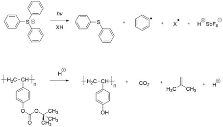
A positive photoresist example, whose solubility would change by the photogenerated acid. The acid deprotects the tert-butoxycarbonyl (t-BOC), inducing the resist from alkali-insoluble to alkali-soluble. This was the first chemically amplified resist used in the semiconductor industry, which was invented by Ito, Willson, and Frechet in 1982.An example of single-component positive photoresist
A positive photoresist is a type of photoresist in which a portion is exposed to light and becomes soluble to the photoresist developer. The unexposed portion of the photoresist remains insoluble in the photoresist developer.
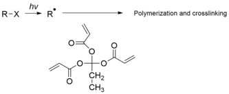
A crosslinking of a polyisoprene rubber by a photoreactive biazide as negative photoresistA radical induced polymerization and crosslinking of an acrylate monomer as negative photoresist
A negative photoresist is a type of photoresist in which the portion of the photoresist that is exposed to light becomes insoluble in the photoresist developer. The unexposed portion of the photoresist is dissolved by the photoresist developer.
Based on cyclized polyisoprene (rubber)
variety of sensitizers (only a few% by weight)
free radical initiated photo cross-linking of polymers
Issues:
potential oxygen inhibition
swelling during development
long narrow lines can become wavy
swelling is an issue for high-resolution patterning
MTF (modulation transfer function is the ratio of image intensity modulation and object intensity modulation and it is a parameter that indicates the capability of an optical system.
Differences between positive and negative resist
The following table[7] is based on generalizations which are generally accepted in the microelectromechanical systems (MEMS) fabrication industry.
Characteristic
Positive
Negative
Adhesion to silicon
Fair
Excellent
Relative cost
More expensive
Less expensive
Developer base
Aqueous
Organic
Solubility in the developer
Exposed region is soluble
Exposed region is insoluble
Minimum feature
0.5μm
7nm
Step coverage
Better
Lower
Wet chemical resistance
Fair
Excellent
Classification
Photopolymerization of methyl methacrylate monomers under UV that resulting into polymerPhotolysis of a dizaonaphthoquinone that leads to a much more polar environment, which allows aqueous base to dissolve a Bakelite-type polymer
Based on the chemical structure of photoresists, they can be classified into three types: photopolymeric, photodecomposing, and photocrosslinking photoresist.
Photopolymeric photoresist is a type of photoresist, usually allyl monomer, that generates free radicals when exposed to light, which then initiates the photopolymerization of the monomer to produce a polymer. Photopolymeric photoresists are usually used for negative photoresist, e.g. methyl methacrylate and poly(phthalaldehyde)/PAG blends
Photocrosslinking photoresist is a type of photoresist that could crosslink chain by chain when exposed to light in order to generate an insoluble network. Photocrosslinking photoresists are usually used for negative photoresist.
Chemical structure of SU-8 (a single molecule contains 8 epoxy groups)
Photodecomposing photoresist is a type of photoresist that generates hydrophilic products under light. Photodecomposing photoresists are usually used for positive photoresist. A typical example is azide quinone, e.g. diazonaphthaquinone (DQ).
For self-assembled monolayer (SAM) photoresist, first a SAM is formed on the substrate by self-assembly. Then, this surface covered by SAM is irradiated through a mask, similar to other photoresists, which generates a photo-patterned sample in the irradiated areas. And finally, developer is used to remove the designed part (could be used as both positive or negative photoresist).[8]
Light sources
Absorption at UV and shorter wavelengths
In lithography, decreasing the wavelength of light source is the most efficient way to achieve higher resolution.[9] Photoresists are most commonly used at wavelengths in the ultraviolet spectrum or shorter (<400nm). For example, diazonaphthoquinone (DNQ) absorbs strongly from approximately 300nm to 450nm. The absorption bands can be assigned to n-π* (S0–S1) and π-π* (S1–S2) transitions in the DNQ molecule.[citation needed] In the deep ultraviolet (DUV) spectrum, the π-π* electronic transition in benzene[10] or carbon double-bond chromophores appears at around 200nm.[citation needed] Due to the appearance of more possible absorption transitions involving larger energy differences, the absorption tends to increase with shorter wavelength, or larger photon energy. Photons with energies exceeding the ionization potential of the photoresist (can be as low as 5 eV in condensed solutions)[11] can also release electrons which are capable of additional exposure of the photoresist. From about 5 eV to about 20 eV, photoionization of outer "valence band" electrons is the main absorption mechanism.[12] Above 20 eV, inner electron ionization and Auger transitions become more important. Photon absorption begins to decrease as the X-ray region is approached, as fewer Auger transitions between deep atomic levels are allowed for the higher photon energy. The absorbed energy can drive further reactions and ultimately dissipates as heat. This is associated with the outgassing and contamination from the photoresist.
Electron-beam exposure
Photoresists can also be exposed by electron beams, producing the same results as exposure by light. The main difference is that while photons are absorbed, depositing all their energy at once, electrons deposit their energy gradually, and scatter within the photoresist during this process. As with high-energy wavelengths, many transitions are excited by electron beams, and heating and outgassing are still a concern. The dissociation energy for a C-C bond is 3.6 eV. Secondary electrons generated by primary ionizing radiation have energies sufficient to dissociate this bond, causing scission. In addition, the low-energy electrons have a longer photoresist interaction time due to their lower speed; essentially the electron has to be at rest with respect to the molecule in order to react most strongly via dissociative electron attachment, where the electron comes to rest at the molecule, depositing all its kinetic energy.[13] The resulting scission breaks the original polymer into segments of lower molecular weight, which are more readily dissolved in a solvent, or else releases other chemical species (acids) which catalyze further scission reactions (see the discussion on chemically amplified resists below). It is not common to select photoresists for electron-beam exposure. Electron beam lithography usually relies on resists dedicated specifically to electron-beam exposure.
Physical, chemical, and optical properties of photoresists influence their selection for different processes.[14] The primary properties of the photoresist are resolution capability, process dose and focus latitude s required for curing, and resistance to reactive ion etching.[15]:966[16] Other key properties are sensitivity, compatibility with tetramethylammonium hydroxide (TMAH), adhesion, environmental stability, and shelf life.[15]:966[16]
Resolution
Resolution is the ability to differ the neighboring features on the substrate. Critical dimension (CD) is a main measure of resolution. The smaller the CD is, the higher resolution would be.
Contrast
Contrast is the difference from exposed portion to unexposed portion. The higher the contrast is, the more obvious the difference between exposed and unexposed portions would be.
Sensitivity
Sensitivity is the minimum energy that is required to generate a well-defined feature in the photoresist on the substrate, measured in mJ/cm2. The sensitivity of a photoresist is important when using deep ultraviolet (DUV) or extreme-ultraviolet (EUV).
Viscosity
Viscosity is a measure of the internal friction of a fluid, affecting how easily it will flow. When it is needed to produce a thicker layer, a photoresist with higher viscosity will be preferred.
Adherence
Adherence is the adhesive strength between photoresist and substrate. If the resist comes off the substrate, some features will be missing or damaged.
Etching resistance
Anti-etching is the ability of a photoresist to resist the high temperature, different pH environment or the ion bombardment in the process of post-modification.
Surface tension
Surface tension is the tension that induced by a liquid tended to minimize its surface area, which is caused by the attraction of the particles in the surface layer. In order to better wet the surface of substrate, photoresists are required to possess relatively low surface tension.
Chemical amplification
Photoresists used in production for DUV and shorter wavelengths require the use of chemical amplification to increase the sensitivity to the exposure energy. This is done in order to combat the larger absorption at shorter wavelengths. Chemical amplification is also often used in electron-beam exposures to increase the sensitivity to the exposure dose. In the process, acids released by the exposure radiation diffuse during the post-exposure bake step. These acids render surrounding polymer soluble in developer. A single acid molecule can catalyze many such 'deprotection' reactions; hence, fewer photons or electrons are needed.[17] Acid diffusion is important not only to increase photoresist sensitivity and throughput, but also to limit line edge roughness due to shot noise statistics.[18] However, the acid diffusion length is itself a potential resolution limiter.[19] In addition, too much diffusion reduces chemical contrast, leading again to more roughness.[18]
The following reactions are an example of commercial chemically amplified photoresists in use today:
The e− represents a solvated electron, or a freed electron that may react with other constituents of the solution. It typically travels a distance on the order of many nanometers before being contained;[22][23] such a large travel distance is consistent with the release of electrons through thick oxide in UV EPROM in response to ultraviolet light. This parasitic exposure would degrade the resolution of the photoresist; for 193nm the optical resolution is the limiting factor anyway, but for electron beam lithography or EUVL it is the electron range that determines the resolution rather than the optics.
One very common positive photoresist used with the I, G and H-lines from a mercury-vapor lamp is based on a mixture of diazonaphthoquinone (DNQ) and novolac resin (a phenol formaldehyde resin). DNQ inhibits the dissolution of the novolac resin, but upon exposure to light, the dissolution rate increases even beyond that of pure novolac. The mechanism by which unexposed DNQ inhibits novolac dissolution is not well understood, but is believed to be related to hydrogen bonding (or more exactly diazocoupling in the unexposed region). DNQ-novolac resists are developed by dissolution in a basic solution (usually 0.26N tetramethylammonium hydroxide (TMAH) in water).
Epoxy-based resists
One very common negative photoresist is based on epoxy-based oligomer. The common product name is SU-8 photoresist, and it was originally invented by IBM, but is now sold by Microchem and Gersteltec. One unique property of SU-8 is that it is very difficult to strip. As such, it is often used in applications where a permanent resist pattern (one that is not strippable, and can even be used in harsh temperature and pressure environments) is needed for a device.[24] Mechanism of epoxy-based polymer is shown in 1.2.3 SU-8. SU-8 is prone to swelling at smaller feature sizes, which has led to the development of small-molecule alternatives that are capable of obtaining higher resolutions than SU-8.[25]
Off-stoichiometry thiol-enes(OSTE) polymer
In 2016, OSTE Polymers were shown to possess a unique photolithography mechanism, based on diffusion-induced monomer depletion, which enables high photostructuring accuracy. The OSTE polymer material was originally invented at the KTH Royal Institute of Technology, but is now sold by Mercene Labs. Whereas the material has properties similar to those of SU8, OSTE has the specific advantage that it contains reactive surface molecules, which make this material attractive for microfluidic or biomedical applications.[14]
Hydrogen silsesquioxane (HSQ)
HSQ is a common negative resist for e-beam, but also useful for photolithography. Originally invented by Dow Corning (1970),[26] and now produced (2017) by Applied Quantum Materials Inc. (AQM). Unlike other negative resists, HSQ is inorganic and metal-free. Therefore, exposed HSQ provides a low dielectric constant (low-k) Si-rich oxide. A comparative study against other photoresists was reported in 2015 (Dow Corning HSQ).[27]
Applications
Creating the PDMS masterrightInking and contact process
Microcontact printing
Microcontact printing was described by Whitesides Group in 1993. Generally, in this techniques, an elastomeric stamp is used to generate two-dimensional patterns, through printing the “ink” molecules onto the surface of a solid substrate.[28]
Steps for microcontact printing: 1) A scheme for the creation of a polydimethylsiloxane (PDMS) master stamp. 2) A scheme of the inking and contact process of microprinting lithography.
Printed circuit boards
The manufacture of printed circuit boards is one of the most important uses of photoresist. Photolithography allows the complex wiring of an electronic system to be rapidly, economically, and accurately reproduced as if run off a printing press. The general process is applying photoresist, exposing image to ultraviolet rays, and then etching to remove the copper-clad substrate.[29]
A printed circuit board-4276
Patterning and etching of substrates
This includes specialty photonics materials, MicroElectro-Mechanical Systems (MEMS), glass printed circuit boards, and other micropatterning tasks. Photoresist tends not to be etched by solutions with a pH greater than 3.[30]
A micro-electrical-mechanical cantilever inproduced by photoetching
Microelectronics
This application, mainly applied to silicon wafers and silicon integrated circuits is the most developed of the technologies and the most specialized in the field.[31]
↑Madou, Marc (2002-03-13). Fundamentals of Microfabrication. CRC Press. ISBN978-0-8493-0826-0.
↑Huang, Jingyu; Dahlgren, David A.; Hemminger, John C. (1994-03-01). "Photopatterning of Self-Assembled Alkanethiolate Monolayers on Gold: A Simple Monolayer Photoresist Utilizing Aqueous Chemistry". Langmuir. 10 (3): 626–628. doi:10.1021/la00015a005. ISSN0743-7463.
↑Bratton, Daniel; Yang, Da; Dai, Junyan; Ober, Christopher K. (2006-02-01). "Recent progress in high resolution lithography". Polymers for Advanced Technologies. 17 (2): 94–103. doi:10.1002/pat.662. ISSN1099-1581. S2CID55877239.
↑Ishii, Hiroyuki; Usui, Shinji; Douki, Katsuji; Kajita, Toru; Chawanya, Hitoshi; Shimokawa, Tsutomu (2000-01-01). Houlihan, Francis M (ed.). "Design and lithographic performances of 193-specific photoacid generators". Advances in Resist Technology and Processing XVII. 3999: 1120–1127. Bibcode:2000SPIE.3999.1120I. doi:10.1117/12.388276. S2CID98281255.
↑Braun, M; Gruber, F; Ruf, M. -W; Kumar, S. V. K; Illenberger, E; Hotop, H (2006). "IR photon enhanced dissociative electron attachment to SF6: Dependence on photon, vibrational, and electron energy". Chemical Physics. 329 (1–3): 148. Bibcode:2006CP....329..148B. doi:10.1016/j.chemphys.2006.07.005.
↑U.S. patent 4,491,628 "Positive and Negative Working Resist Compositions with Acid-Generating Photoinitiator and Polymer with Acid-Labile Groups Pendant From Polymer Backbone" J.M.J. Fréchet, H. Ito and C.G. Willson 1985.Archived 2019-02-02 at the Wayback Machine
↑Chochos, Ch.L.; Ismailova, E. (2009). "Hyperbranched Polymers for Photolithographic Applications – Towards Understanding the Relationship between Chemical Structure of Polymer Resin and Lithographic Performances". Advanced Materials. 21 (10–11): 1121. Bibcode:2009AdM....21.1121C. doi:10.1002/adma.200801715. S2CID95710610.
12S. Tagawa; etal. (2000). Houlihan, Francis M. (ed.). "Radiation and photochemistry of onium salt acid generators in chemically amplified resists". Proc. SPIE. Advances in Resist Technology and Processing XVII. 3999: 204. Bibcode:2000SPIE.3999..204T. doi:10.1117/12.388304. S2CID95525894.
↑Wang, Xue-Bin; Ferris, Kim; Wang, Lai-Sheng (2000). "Photodetachment of Gaseous Multiply Charged Anions, Copper Phthalocyanine Tetrasulfonate Tetraanion: Tuning Molecular Electronic Energy Levels by Charging and Negative Electron Binding". The Journal of Physical Chemistry A. 104 (1): 25–33. Bibcode:2000JPCA..104...25W. doi:10.1021/jp9930090.
↑Lu, Hong; Long, Frederick H.; Eisenthal, K. B. (1990). "Femtosecond studies of electrons in liquids". Journal of the Optical Society of America B. 7 (8): 1511. Bibcode:1990JOSAB...7.1511L. doi:10.1364/JOSAB.7.001511.
↑Lukin, L; Balakin, Alexander A. (2001). "Thermalization of low energy electrons in liquid methylcyclohexane studied by the photoassisted ion pair separation technique". Chemical Physics. 265 (1): 87–104. Bibcode:2001CP....265...87L. doi:10.1016/S0301-0104(01)00260-9.
↑DeForest, William S (1975). Photoresist: materials and processes. McGraw-Hill Companies.
↑Montrose, Mark I (1999). The Electronic Packaging Handbook. CRC Press.
↑Novak, R.E (2000). Cleaning Technology in Semiconductor Device Manufacturing. Electrochemical Society Inc. ISBN978-1566772594.
↑Silicon photonics. Springer Science & Business Media. 2004.
This page is based on this Wikipedia article Text is available under the CC BY-SA 4.0 license; additional terms may apply. Images, videos and audio are available under their respective licenses.