Celeron is a series of IA-32 and x86-64 computer microprocessors targeted at low-cost personal computers, manufactured by Intel from 1998 until 2023.

The Pentium III brand refers to Intel's 32-bit x86 desktop and mobile CPUs based on the sixth-generation P6 microarchitecture introduced on February 28, 1999. The brand's initial processors were very similar to the earlier Pentium II-branded processors. The most notable differences were the addition of the Streaming SIMD Extensions (SSE) instruction set, and the introduction of a controversial serial number embedded in the chip during manufacturing.

Xeon is a brand of x86 microprocessors designed, manufactured, and marketed by Intel, targeted at the non-consumer workstation, server, and embedded markets. It was introduced in June 1998. Xeon processors are based on the same architecture as regular desktop-grade CPUs, but have advanced features such as support for error correction code (ECC) memory, higher core counts, more PCI Express lanes, support for larger amounts of RAM, larger cache memory and extra provision for enterprise-grade reliability, availability and serviceability (RAS) features responsible for handling hardware exceptions through the Machine Check Architecture (MCA). They are often capable of safely continuing execution where a normal processor cannot due to these extra RAS features, depending on the type and severity of the machine-check exception (MCE). Some also support multi-socket systems with two, four, or eight sockets through use of the Ultra Path Interconnect (UPI) bus, which replaced the older QuickPath Interconnect (QPI) bus.

Mini-ITX is a 170 mm × 170 mm motherboard form factor developed by VIA Technologies in 2001. Mini-ITX motherboards have been traditionally used in small-configured computer systems. Originally, Mini-ITX was a niche standard designed for fanless cooling with a low power consumption architecture, which made them useful for home theater PC systems, where fan noise can detract from the cinema experience.

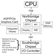
Pentium D is a range of desktop 64-bit x86-64 processors based on the NetBurst microarchitecture, which is the dual-core variant of the Pentium 4 manufactured by Intel. Each CPU comprised two cores. The brand's first processor, codenamed Smithfield and manufactured on the 90 nm process, was released on May 25, 2005, followed by the 65 nm Presler nine months later. The core implementation on the 90 nm Smithfield and later 65 nm Presler are designed differently but are functionally the same. The 90 nm Smithfield contains a single die, with two adjoined but functionally separate CPU cores cut from the same wafer. The later 65 nm Presler utilized a multi-chip module package, where two discrete dies each containing a single core reside on the CPU substrate. Neither the 90 nm Smithfield nor the 65 nm Presler were capable of direct core to core communication, relying instead on the northbridge link to send information between the two cores.
In the fields of digital electronics and computer hardware, multi-channel memory architecture is a technology that increases the data transfer rate between the DRAM memory and the memory controller by adding more channels of communication between them. Theoretically, this multiplies the data rate by exactly the number of channels present. Dual-channel memory employs two channels. The technique goes back as far as the 1960s having been used in IBM System/360 Model 91 and in CDC 6600.
The Intel Core microarchitecture is a multi-core processor microarchitecture launched by Intel in mid-2006. It is a major evolution over the Yonah, the previous iteration of the P6 microarchitecture series which started in 1995 with Pentium Pro. It also replaced the NetBurst microarchitecture, which suffered from high power consumption and heat intensity due to an inefficient pipeline designed for high clock rate. In early 2004 the new version of NetBurst (Prescott) needed very high power to reach the clocks it needed for competitive performance, making it unsuitable for the shift to dual/multi-core CPUs. On May 7, 2004 Intel confirmed the cancellation of the next NetBurst, Tejas and Jayhawk. Intel had been developing Merom, the 64-bit evolution of the Pentium M, since 2001, and decided to expand it to all market segments, replacing NetBurst in desktop computers and servers. It inherited from Pentium M the choice of a short and efficient pipeline, delivering superior performance despite not reaching the high clocks of NetBurst.
Double Data Rate 3 Synchronous Dynamic Random-Access Memory is a type of synchronous dynamic random-access memory (SDRAM) with a high bandwidth interface, and has been in use since 2007. It is the higher-speed successor to DDR and DDR2 and predecessor to DDR4 synchronous dynamic random-access memory (SDRAM) chips. DDR3 SDRAM is neither forward nor backward compatible with any earlier type of random-access memory (RAM) because of different signaling voltages, timings, and other factors.
The nForce 600 chipset was released in the first half of November 2006, coinciding with the GeForce 8 series launch on November 8, 2006. The nForce 600 supports Intel's LGA 775 socket and AMD's Quad FX platform and replaces the nForce 500 series.
The AMD 700 chipset series is a set of chipsets designed by ATI for AMD Phenom processors to be sold under the AMD brand. Several members were launched in the end of 2007 and the first half of 2008, others launched throughout the rest of 2008.
The AMD 690 chipset series is an integrated graphics chipset family which was developed and manufactured by AMD subsidiary ATI for both AMD and Intel platforms focusing on both desktop and mobile computing markets. The corresponding chipset for the Intel platform has a marketing name of Radeon Xpress 1200 series.
Skulltrail is an enthusiast gaming platform released by Intel on February 19, 2008. It is based on Intel's 5400 "Seaburg" workstation chipset. The primary difference between Skulltrail and Intel's current and past enthusiast chipsets is a dual CPU socket design that allows two processors to operate on the same motherboard. Therefore, Skulltrail can operate eight processing cores on one system. The platform supports two Core 2 Extreme QX9775 processors, which operate at 3.2 GHz.
The P35 Express is a mainstream desktop computer chipset from Intel released in June 2007, although motherboards featuring the chipset were available a month earlier. The P35 Express chipset supports Intel's LGA 775 socket and Core 2 Duo and Quad processors, and is also known to support 45 nm Wolfdale/Yorkfield dual and quad core CPUs. Theoretically, Intel also dropped support for Intel's Pentium 4 and Pentium D processors with this chipset although late Pentium 4 processors, including both the 32-bit-only (5x0) and the 32-bit/64-bit (5x1), and a few others, were fully supported.

Phenom II is a family of AMD's multi-core 45 nm processors using the AMD K10 microarchitecture, succeeding the original Phenom. Advanced Micro Devices released the Socket AM2+ version of Phenom II in December 2008, while Socket AM3 versions with DDR3 support, along with an initial batch of triple- and quad-core processors were released on February 9, 2009. Dual-processor systems require Socket F+ for the Quad FX platform. The next-generation Phenom II X6 was released on April 27, 2010.

Conroe is the code name for many Intel processors sold as Core 2 Duo, Xeon, Pentium Dual-Core and Celeron. It was the first desktop processor to be based on the Core microarchitecture, replacing the NetBurst microarchitecture based Cedar Mill processor. It has product code 80557, which is shared with Allendale and Conroe-L that are very similar but have a smaller L2 cache. Conroe-L has only one processor core and a new CPUID model. The mobile version of Conroe is Merom, the dual-socket server version is Woodcrest, the quad-core desktop version is Kentsfield and the quad-core dual-socket version is Clovertown. Conroe was replaced by the 45 nm Wolfdale processor.
Bloomfield is the code name for Intel high-end desktop processors sold as Core i7-9xx and single-processor servers sold as Xeon 35xx., in almost identical configurations, replacing the earlier Yorkfield processors. The Bloomfield core is closely related to the dual-processor Gainestown, which has the same CPUID value of 0106Ax and which uses the same socket. Bloomfield uses a different socket than the later Lynnfield and Clarksfield processors based on the same 45 nm Nehalem microarchitecture, even though some of these share the same Intel Core i7 brand.

LGA 1155, also called Socket H2, is a zero insertion force flip-chip land grid array (LGA) CPU socket designed by Intel for their CPUs based on the Sandy Bridge and Ivy Bridge microarchitectures.
