DDR2 SDRAM

Last updated
DDR2 SDRAM
Double Data Rate 2 Synchronous Dynamic Random-Access Memory
Type of RAM
Swissbit 2GB PC2-5300U-555.jpg
Front and back of a 2GB PC2-5300 DDR2 RAM module for desktop PCs (DIMM)
Developer Samsung [1]
JEDEC
Type Synchronous dynamic random-access memory
Generation2nd generation
Release dateSeptember 2003 (September 2003)
Standards
  • DDR2-400 (PC2-3200)
  • DDR2-533 (PC2-4266)
  • DDR2-667 (PC2-5333)
  • DDR2-800 (PC2-6400)
  • DDR2-1066 (PC2-8500)
Clock rate 100–266 MHz
Cycle time10–3.75 ns
Bus clock rate200–533 MHz
Transfer rate 400–1066 MT/s
Voltage 1.8 V
Predecessor DDR SDRAM
Successor DDR3 SDRAM

Double Data Rate 2 Synchronous Dynamic Random-Access Memory (DDR2 SDRAM) is a double data rate (DDR) synchronous dynamic random-access memory (SDRAM) interface. It is a JEDEC standard (JESD79-2); first published in September 2003. [2] DDR2 succeeded the original DDR SDRAM specification, and was itself succeeded by DDR3 SDRAM in 2007. DDR2 DIMMs are neither forward compatible with DDR3 nor backward compatible with DDR.

Contents

In addition to double pumping the data bus as in DDR SDRAM (transferring data on the rising and falling edges of the bus clock signal), DDR2 allows higher bus speed and requires lower power by running the internal clock at half the speed of the data bus. The two factors combine to produce a total of four data transfers per internal clock cycle.

Since the DDR2 internal clock runs at half the DDR external clock rate, DDR2 memory operating at the same external data bus clock rate as DDR results in DDR2 being able to provide the same bandwidth but with better latency. Alternatively, DDR2 memory operating at twice the external data bus clock rate as DDR may provide twice the bandwidth with the same latency. The best-rated DDR2 memory modules are at least twice as fast as the best-rated DDR memory modules. The maximum capacity on commercially available DDR2 DIMMs is 8GB, but chipset support and availability for those DIMMs is sparse and more common 2GB per DIMM are used.[ citation needed ] [3]
History

DDR2 SDRAM was first produced by Samsung in 2001. In 2003, the JEDEC standards organization presented Samsung with its Technical Recognition Award for the company's efforts in developing and standardizing DDR2. [1]

DDR2 was officially introduced in the second quarter of 2003 at two initial clock rates: 200 MHz (referred to as PC2-3200) and 266 MHz (PC2-4200). Both performed worse than the original DDR specification due to higher latency, which made total access times longer. However, the original DDR technology tops out at a clock rate around 200 MHz (400 MT/s). Higher performance DDR chips exist, but JEDEC has stated that they will not be standardized. These chips are mostly standard DDR chips that have been tested and rated to be capable of operation at higher clock rates by the manufacturer. Such chips draw significantly more power than slower-clocked chips, but usually offered little or no improvement in real-world performance. DDR2 started to become competitive against the older DDR standard by the end of 2004, as modules with lower latencies became available. [4]

Specification

Overview

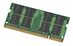
PC2-5300 DDR2 SO-DIMM (for notebooks) Samsung-1GB-DDR2-Laptop-RAM.jpg
PC2-5300 DDR2 SO-DIMM (for notebooks)
Comparison of memory modules for desktop PCs (DIMM) Desktop DDR Memory Comparison.svg
Comparison of memory modules for desktop PCs (DIMM)
Comparison of memory modules for portable/mobile PCs (SO-DIMM) Laptop SODIMM DDR Memory Comparison V2.svg
Comparison of memory modules for portable/mobile PCs (SO-DIMM)

The key difference between DDR2 and DDR SDRAM is the increase in prefetch length. In DDR SDRAM, the prefetch length was two bits for every bit in a word; whereas it is four bits in DDR2 SDRAM. During an access, four bits were read or written to or from a four-bit-deep prefetch queue. This queue received or transmitted its data over the data bus in two data bus clock cycles (each clock cycle transferred two bits of data). Increasing the prefetch length allowed DDR2 SDRAM to double the rate at which data could be transferred over the data bus without a corresponding doubling in the rate at which the DRAM array could be accessed. DDR2 SDRAM was designed with such a scheme to avoid an excessive increase in power consumption.

DDR2's bus frequency is boosted by electrical interface improvements, on-die termination, prefetch buffers and off-chip drivers. However, latency is greatly increased as a trade-off. The DDR2 prefetch buffer is four bits deep, whereas it is two bits deep for DDR. While DDR SDRAM has typical read latencies of between two and three bus cycles, DDR2 may have read latencies between three and nine cycles, although the typical range is between four and six. Thus, DDR2 memory must be operated at twice the data rate to achieve the same latency.

Another cost of the increased bandwidth is the requirement that the chips are packaged in a more expensive and difficult to assemble BGA package as compared to the TSSOP package of the previous memory generations such as DDR SDRAM and SDR SDRAM. This packaging change was necessary to maintain signal integrity at higher bus speeds.

Power savings are achieved primarily due to an improved manufacturing process through die shrinkage, resulting in a drop in operating voltage (1.8 V compared to DDR's 2.5 V). The lower memory clock frequency may also enable power reductions in applications that do not require the highest available data rates.

According to JEDEC [5] the maximum recommended voltage is 1.9 volts and should be considered the absolute maximum when memory stability is an issue (such as in servers or other mission critical devices). In addition, JEDEC states that memory modules must withstand up to 2.3 volts before incurring permanent damage (although they may not actually function correctly at that level).

Chips and modules

For use in computers, DDR2 SDRAM is supplied in DIMMs with 240 pins and a single locating notch. Laptop DDR2 SO-DIMMs have 200 pins and often come identified by an additional S in their designation. DIMMs are identified by their peak transfer capacity (often called bandwidth).

Comparison of DDR2 SDRAM standards
Name Chip Bus Timings
StandardTypeModule Clock rate (MHz)Cycle time (ns) [6] Clock rate (MHz) Transfer rate (MT/s) Bandwidth (MB/s)CL-TRCD-TRP [7] [8] CAS latency (ns)
DDR2-400BPC2-32001001020040032003-3-315
C4-4-420
DDR2-533BPC2-4200*1337.526653342663-3-311.25
C4-4-415
DDR2-667CPC2-5300*166633366753334-4-412
D5-5-515
DDR2-800CPC2-6400200540080064004-4-410
D5-5-512.5
E6-6-615
DDR2-1066EPC2-8500*2663.75533106685336-6-611.25
F7-7-713.125
Relative speed comparison between similar modules
PC-5300PC-6400
5-5-54-4-46-6-65-5-54-4-4
PC2-3200 4-4-4 % %+33%+60% %
PC2-3200 3-3-3 % %=+20% %
PC2-4200 4-4-4 % %=+21% %
PC2-4200 3-3-3 % %−24%−9% %
PC2-5300 5-5-5 % %=+21% %
PC2-5300 4-4-4 % %−19%−3% %
PC2-6400 6-6-6 % %=+20% %
PC2-6400 5-5-5 % %−16%= %
PC2-6400 4-4-4 % %−33%−20% %
PC2-8500 7-7-7 % %−12%+6% %
PC2-8500 6-6-6 % %−25%−9% %

*Some manufacturers label their DDR2 modules as PC2-4300, PC2-5400 or PC2-8600 instead of the respective names suggested by JEDEC. At least one manufacturer has reported this reflects successful testing at a higher-than-standard data rate [9] whilst others simply round up for the name.

Note: DDR2-xxx denotes data transfer rate, and describes raw DDR chips, whereas PC2-xxxx denotes theoretical bandwidth (with the last two digits truncated), and is used to describe assembled DIMMs. Bandwidth is calculated by taking transfers per second and multiplying by eight. This is because DDR2 memory modules transfer data on a bus that is 64 data bits wide, and since a byte comprises 8 bits, this equates to 8 bytes of data per transfer.

DDR2 P vs F Server DIMM's Notch Positions compared DDR2 F 'Fully Buffer' vs 'Parity' notch position.jpg
DDR2 P vs FServer DIMM's Notch Positions compared

In addition to bandwidth and capacity variants, modules can:

  1. Optionally implement ECC, which is an extra data byte lane used for correcting minor errors and detecting major errors for better reliability. Modules with ECC are identified by an additional ECC in their designation. PC2-4200 ECC is a PC2-4200 module with ECC. An additional P can be added at the end of the designation, P standing for parity (ex : PC2-5300P).
  2. Intel (r) 6402 Advanced Memory Buffer Intel (r) 6402 Advanced Memory Buffer..jpg
    Intel ® 6402 Advanced Memory Buffer
    Be "registered" ("buffered"), which improves signal integrity (and hence potentially clock rates and physical slot capacity) by electrically buffering the signals at a cost of an extra clock of increased latency. Those modules are identified by an additional R in their designation, whereas non-registered (a.k.a. "unbuffered") RAM may be identified by an additional U in the designation. PC2-4200R is a registered PC2-4200 module, PC2-4200R ECC is the same module but with additional ECC.
  3. Be aware fully buffered modules, which are designated by F or FB do not have the same notch position as other classes. Fully buffered modules cannot be used with motherboards that are made for registered modules, and the different notch position physically prevents their insertion.

Note:

Backward compatibility

DDR2 DIMMs are not backward compatible with DDR DIMMs. The notch on DDR2 DIMMs is in a different position from DDR DIMMs, and the pin density is higher than DDR DIMMs in desktops. DDR2 is a 240-pin module, DDR is a 184-pin module. Notebooks have 200-pin SO-DIMMs for DDR and DDR2; however, the notch on DDR2 modules is in a slightly different position than on DDR modules.

Higher-speed DDR2 DIMMs can be mixed with lower-speed DDR2 DIMMs, although the memory controller will operate all DIMMs at same speed as the lowest-speed DIMM present.

Relation to GDDR memory

GDDR2, a form of GDDR SDRAM, was developed by Samsung and introduced in July 2002. [10] The first commercial product to claim using the "DDR2" technology was the Nvidia GeForce FX 5800 graphics card. However, this GDDR2 memory used on graphics cards is not DDR2 per se, but rather an early midpoint between DDR and DDR2 technologies. Using "DDR2" to refer to GDDR2 is a colloquial misnomer. In particular, the performance-enhancing doubling of the I/O clock rate is missing. It had severe overheating issues due to the nominal DDR voltages. ATI has since designed the GDDR technology further into GDDR3, which is based on DDR2 SDRAM, though with several additions suited for graphics cards.

GDDR3, GDDR5 and GDDR6 is now commonly used in modern graphics cards and some tablet PCs. However, further confusion has been added to the mix with the appearance of budget and mid-range graphics cards which claim to use "GDDR2". These cards actually use standard DDR2 chips designed for use as main system memory although operating with higher latencies to achieve higher clockrates. These chips cannot achieve the clock rates of GDDR3 but are inexpensive and fast enough to be used as memory on mid-range cards.

See also

Related Research Articles

<span class="mw-page-title-main">DDR SDRAM</span> Type of computer memory

Double Data Rate Synchronous Dynamic Random-Access Memory is a double data rate (DDR) synchronous dynamic random-access memory (SDRAM) class of memory integrated circuits used in computers. DDR SDRAM, also retroactively called DDR1 SDRAM, has been superseded by DDR2 SDRAM, DDR3 SDRAM, DDR4 SDRAM and DDR5 SDRAM. None of its successors are forward or backward compatible with DDR1 SDRAM, meaning DDR2, DDR3, DDR4 and DDR5 memory modules will not work on DDR1-equipped motherboards, and vice versa.

<span class="mw-page-title-main">Synchronous dynamic random-access memory</span> Type of computer memory

Synchronous dynamic random-access memory is any DRAM where the operation of its external pin interface is coordinated by an externally supplied clock signal.

<span class="mw-page-title-main">DIMM</span> Computer memory module

A DIMM, commonly called a RAM stick, comprises a series of dynamic random-access memory integrated circuits. These memory modules are mounted on a printed circuit board and designed for use in personal computers, workstations, printers, and servers. They are the predominant method for adding memory into a computer system. The vast majority of DIMMs are standardized through JEDEC standards, although there are proprietary DIMMs. DIMMs come in a variety of speeds and sizes, but generally are one of two lengths - PC which are 133.35 mm (5.25 in) and laptop (SO-DIMM) which are about half the size at 67.60 mm (2.66 in).

Rambus DRAM (RDRAM), and its successors Concurrent Rambus DRAM (CRDRAM) and Direct Rambus DRAM (DRDRAM), are types of synchronous dynamic random-access memory (SDRAM) developed by Rambus from the 1990s through to the early 2000s. The third-generation of Rambus DRAM, DRDRAM was replaced by XDR DRAM. Rambus DRAM was developed for high-bandwidth applications and was positioned by Rambus as replacement for various types of contemporary memories, such as SDRAM.

<span class="mw-page-title-main">Double data rate</span>

In computing, a computer bus operating with double data rate (DDR) transfers data on both the rising and falling edges of the clock signal. This is also known as double pumped, dual-pumped, and double transition. The term toggle mode is used in the context of NAND flash memory.

<span class="mw-page-title-main">Registered memory</span>

Registeredmemory modules have a register between the DRAM modules and the system's memory controller. They place less electrical load on the memory controller and allow single systems to remain stable with more memory modules than they would have otherwise. When compared with registered memory, conventional memory is usually referred to as unbuffered memory or unregistered memory. When manufactured as a dual in-line memory module (DIMM), a registered memory module is called an RDIMM, while unregistered memory is called UDIMM or simply DIMM.

In computing, serial presence detect (SPD) is a standardized way to automatically access information about a memory module. Earlier 72-pin SIMMs included five pins that provided five bits of parallel presence detect (PPD) data, but the 168-pin DIMM standard changed to a serial presence detect to encode much more information.

Double Data Rate 3 Synchronous Dynamic Random-Access Memory is a type of synchronous dynamic random-access memory (SDRAM) with a high bandwidth interface, and has been in use since 2007. It is the higher-speed successor to DDR and DDR2 and predecessor to DDR4 synchronous dynamic random-access memory (SDRAM) chips. DDR3 SDRAM is neither forward nor backward compatible with any earlier type of random-access memory (RAM) because of different signaling voltages, timings, and other factors.

<span class="mw-page-title-main">Fully Buffered DIMM</span>

Fully Buffered DIMM is a memory technology that can be used to increase reliability and density of memory systems. Unlike the parallel bus architecture of traditional DRAMs, an FB-DIMM has a serial interface between the memory controller and the advanced memory buffer (AMB). Conventionally, data lines from the memory controller have to be connected to data lines in every DRAM module, i.e. via multidrop buses. As the memory width increases together with the access speed, the signal degrades at the interface between the bus and the device. This limits the speed and memory density, so FB-DIMMs take a different approach to solve the problem.

GDDR4 SDRAM, an abbreviation for Graphics Double Data Rate 4 Synchronous Dynamic Random-Access Memory, is a type of graphics card memory (SGRAM) specified by the JEDEC Semiconductor Memory Standard. It is a rival medium to Rambus's XDR DRAM. GDDR4 is based on DDR3 SDRAM technology and was intended to replace the DDR2-based GDDR3, but it ended up being replaced by GDDR5 within a year.

<span class="mw-page-title-main">GDDR5 SDRAM</span> Type of high performance DRAM graphics card memory

Graphics Double Data Rate 5 Synchronous Dynamic Random-Access Memory is a type of synchronous graphics random-access memory (SGRAM) with a high bandwidth interface designed for use in graphics cards, game consoles, and high-performance computing. It is a type of GDDR SDRAM.

The JEDEC memory standards are the specifications for semiconductor memory circuits and similar storage devices promulgated by the Joint Electron Device Engineering Council (JEDEC) Solid State Technology Association, a semiconductor trade and engineering standardization organization.

Graphics DDR SDRAM is a type of synchronous dynamic random-access memory (SDRAM) specifically designed for applications requiring high bandwidth, e.g. graphics processing units (GPUs). GDDR SDRAM is distinct from the more widely known types of DDR SDRAM, such as DDR4 and DDR5, although they share some of the same features—including double data rate data transfers. As of 2023, GDDR SDRAM has been succeeded by GDDR2, GDDR3, GDDR4, GDDR5, GDDR5X, GDDR6, GDDR6X and GDDR6W.

Memory timings or RAM timings describe the timing information of a memory module or the onboard LPDDRx. Due to the inherent qualities of VLSI and microelectronics, memory chips require time to fully execute commands. Executing commands too quickly will result in data corruption and results in system instability. With appropriate time between commands, memory modules/chips can be given the opportunity to fully switch transistors, charge capacitors and correctly signal back information to the memory controller. Because system performance depends on how fast memory can be used, this timing directly affects the performance of the system.

Double Data Rate 4 Synchronous Dynamic Random-Access Memory is a type of synchronous dynamic random-access memory with a high bandwidth interface.

<span class="mw-page-title-main">LPDDR</span> Computer hardware

Low-Power Double Data Rate (LPDDR), also known as LPDDR SDRAM, is a type of synchronous dynamic random-access memory that consumes less power and is targeted for mobile computers and devices such as mobile phones. Older variants are also known as Mobile DDR, and abbreviated as mDDR.

<span class="mw-page-title-main">GDDR3 SDRAM</span> Type of graphics card memory

GDDR3 SDRAM is a type of DDR SDRAM specialized for graphics processing units (GPUs) offering less access latency and greater device bandwidths. Its specification was developed by ATI Technologies in collaboration with DRAM vendors including Elpida Memory, Hynix Semiconductor, Infineon and Micron. It was later adopted as a JEDEC standard.

<span class="mw-page-title-main">DDR5 SDRAM</span> Fifth generation of double-data-rate synchronous dynamic random-access memory

Double Data Rate 5 Synchronous Dynamic Random-Access Memory is a type of synchronous dynamic random-access memory. Compared to its predecessor DDR4 SDRAM, DDR5 was planned to reduce power consumption, while doubling bandwidth. The standard, originally targeted for 2018, was released on July 14, 2020.

<span class="mw-page-title-main">High Bandwidth Memory</span> Type of memory used on processors that require high speed memory

High Bandwidth Memory (HBM) is a high-speed computer memory interface for 3D-stacked synchronous dynamic random-access memory (SDRAM) initially from Samsung, AMD and SK Hynix. It is used in conjunction with high-performance graphics accelerators, network devices, high-performance datacenter AI ASICs and FPGAs and in some supercomputers. The first HBM memory chip was produced by SK Hynix in 2013, and the first devices to use HBM were the AMD Fiji GPUs in 2015.

References

  1. 1 2 "Samsung Demonstrates World's First DDR 3 Memory Prototype". Phys.org . 17 February 2005. Retrieved 23 June 2019.
  2. "JEDEC Publishes DDR2 Standard" (PDF). 2003-09-12. Archived from the original (PDF) on 2003-12-04.
  3. https://media-www.micron.com/-/media/client/global/documents/products/data-sheet/modules/parity_rdimm/htf36c256_512_1gx72pz.pdf?rev=e8e3928f09794d61809f92abf36bfb24 [ bare URL PDF ]
  4. Ilya Gavrichenkov. "DDR2 vs. DDR: Revenge gained". X-bit Laboratories. Archived from the original on 2006-11-21.
  5. JEDEC JESD 208 (section 5, tables 15 and 16)
  6. Cycle time is the inverse of the I/O bus clock frequency; e.g., 1/(100 MHz) = 10 ns per clock cycle.
  7. "DDR2 SDRAM SPECIFICATION" (PDF). JESD79-2E. JEDEC. April 2008: 78. Retrieved 2009-03-14.{{cite journal}}: Cite journal requires |journal= (help)
  8. "SPECIALITY DDR2-1066 SDRAM" (PDF). JEDEC. November 2007: 70. Retrieved 2009-03-14.{{cite journal}}: Cite journal requires |journal= (help)
  9. Mushkin PC2-5300 vs. Corsair PC2-5400
  10. "Samsung Electronics Announces JEDEC-Compliant 256Mb GDDR2 for 3D Graphics". Samsung Electronics . Samsung. 23 August 2003. Retrieved 26 June 2019.

Further reading

Note**: JEDEC website requires registration ($2,500 membership) for viewing or downloading of these documents: http://www.jedec.org/standards-documents