Related Research Articles

Synchronous dynamic random-access memory is any DRAM where the operation of its external pin interface is coordinated by an externally supplied clock signal.
HyperTransport (HT), formerly known as Lightning Data Transport, is a technology for interconnection of computer processors. It is a bidirectional serial/parallel high-bandwidth, low-latency point-to-point link that was introduced on April 2, 2001. The HyperTransport Consortium is in charge of promoting and developing HyperTransport technology.
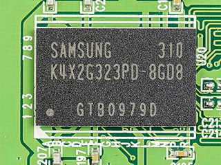
Double Data Rate 3 Synchronous Dynamic Random-Access Memory is a type of synchronous dynamic random-access memory (SDRAM) with a high bandwidth interface, and has been in use since 2007. It is the higher-speed successor to DDR and DDR2 and predecessor to DDR4 synchronous dynamic random-access memory (SDRAM) chips. DDR3 SDRAM is neither forward nor backward compatible with any earlier type of random-access memory (RAM) because of different signaling voltages, timings, and other factors.

A multi-chip module (MCM) is generically an electronic assembly where multiple integrated circuits, semiconductor dies and/or other discrete components are integrated, usually onto a unifying substrate, so that in use it can be treated as if it were a larger IC. Other terms for MCM packaging include "heterogeneous integration" or "hybrid integrated circuit". The advantage of using MCM packaging is it allows a manufacturer to use multiple components for modularity and/or to improve yields over a conventional monolithic IC approach.
GDDR4 SDRAM, an abbreviation for Graphics Double Data Rate 4 Synchronous Dynamic Random-Access Memory, is a type of graphics card memory (SGRAM) specified by the JEDEC Semiconductor Memory Standard. It is a rival medium to Rambus's XDR DRAM. GDDR4 is based on DDR3 SDRAM technology and was intended to replace the DDR2-based GDDR3, but it ended up being replaced by GDDR5 within a year.

Graphics Double Data Rate 5 Synchronous Dynamic Random-Access Memory is a type of synchronous graphics random-access memory (SGRAM) with a high bandwidth interface designed for use in graphics cards, game consoles, and high-performance computing. It is a type of GDDR SDRAM.

In electronic engineering, a through-silicon via (TSV) or through-chip via is a vertical electrical connection (via) that passes completely through a silicon wafer or die. TSVs are high-performance interconnect techniques used as an alternative to wire-bond and flip chips to create 3D packages and 3D integrated circuits. Compared to alternatives such as package-on-package, the interconnect and device density is substantially higher, and the length of the connections becomes shorter.
A three-dimensional integrated circuit is a MOS integrated circuit (IC) manufactured by stacking as many as 16 or more ICs and interconnecting them vertically using, for instance, through-silicon vias (TSVs) or Cu-Cu connections, so that they behave as a single device to achieve performance improvements at reduced power and smaller footprint than conventional two dimensional processes. The 3D IC is one of several 3D integration schemes that exploit the z-direction to achieve electrical performance benefits in microelectronics and nanoelectronics.
Double Data Rate 4 Synchronous Dynamic Random-Access Memory is a type of synchronous dynamic random-access memory with a high bandwidth interface.
The SPARC64 V (Zeus) is a SPARC V9 microprocessor designed by Fujitsu. The SPARC64 V was the basis for a series of successive processors designed for servers, and later, supercomputers.
Low-Power Double Data Rate (LPDDR), also known as LPDDR SDRAM, is a type of synchronous dynamic random-access memory (SDRAM) that consumes less power than other random access memory designs and is thus targeted for mobile computing devices such as laptop computers and smartphones. Older variants are also known as Mobile DDR, and abbreviated as mDDR.
Terabit Ethernet (TbE) is Ethernet with speeds above 100 Gigabit Ethernet. The 400 Gigabit Ethernet and 200 Gigabit Ethernet standard developed by the IEEE P802.3bs Task Force using broadly similar technology to 100 Gigabit Ethernet was approved on December 6, 2017. On February 16, 2024 the 800 Gigabit Ethernet standard developed by the IEEE P802.3df Task Force was approved.

POWER8 is a family of superscalar multi-core microprocessors based on the Power ISA, announced in August 2013 at the Hot Chips conference. The designs are available for licensing under the OpenPOWER Foundation, which is the first time for such availability of IBM's highest-end processors.

Double Data Rate 5 Synchronous Dynamic Random-Access Memory is a type of synchronous dynamic random-access memory. Compared to its predecessor DDR4 SDRAM, DDR5 was planned to reduce power consumption, while doubling bandwidth. The standard, originally targeted for 2018, was released on July 14, 2020.
High Bandwidth Memory (HBM) is a computer memory interface for 3D-stacked synchronous dynamic random-access memory (SDRAM) initially from Samsung, AMD and SK Hynix. It is used in conjunction with high-performance graphics accelerators, network devices, high-performance datacenter AI ASICs, as on-package cache in CPUs and on-package RAM in upcoming CPUs, and FPGAs and in some supercomputers. The first HBM memory chip was produced by SK Hynix in 2013, and the first devices to use HBM were the AMD Fiji GPUs in 2015.
Multi-Channel DRAM or MCDRAM is a 3D-stacked DRAM that is used in the Intel Xeon Phi processor codenamed Knights Landing. It is a version of Hybrid Memory Cube developed in partnership with Micron Technology, and a competitor to High Bandwidth Memory.
Coherent Accelerator Processor Interface (CAPI), is a high-speed processor expansion bus standard for use in large data center computers, initially designed to be layered on top of PCI Express, for directly connecting central processing units (CPUs) to external accelerators like graphics processing units (GPUs), ASICs, FPGAs or fast storage. It offers low latency, high speed, direct memory access connectivity between devices of different instruction set architectures.
Graphics Double Data Rate 6 Synchronous Dynamic Random-Access Memory is a type of synchronous graphics random-access memory (SGRAM) with a high bandwidth, "double data rate" interface, designed for use in graphics cards, game consoles, and high-performance computing. It is a type of GDDR SDRAM, and is the successor to GDDR5. Just like GDDR5X it uses QDR in reference to the write command clock (WCK) and ODR in reference to the command clock (CK).
Graphics Double Data Rate 7 Synchronous Dynamic Random-Access Memory is a type of synchronous graphics random-access memory (SGRAM) specified by the JEDEC Semiconductor Memory Standard, with a high bandwidth, "double data rate" interface, designed for use in graphics cards, game consoles, and high-performance computing. It is a type of GDDR SDRAM, and is the successor to GDDR6.
References
- ↑ Kada, Morihiro (2015). "Research and Development History of Three-Dimensional Integration Technology" (PDF). Three-Dimensional Integration of Semiconductors: Processing, Materials, and Applications. Springer. pp. 15–6. ISBN 9783319186757. Archived from the original (PDF) on 23 October 2021. Retrieved 19 July 2019.
- 1 2 Micron Reinvents DRAM Memory, Linley Group, Jag Bolaria, 12 September 2011
- 1 2 Mearian, Lucas (25 September 2013). "Micron ships Hybrid Memory Cube that boosts DRAM 15X". computerworld.com. Computerworld. Archived from the original on 11 October 2014. Retrieved 4 November 2014.
- ↑ Microsoft backs Hybrid Memory Cube tech // by Gareth Halfacree, bit-tech, 9 May 2012
- ↑ "About Us". Hybrid Memory Cube Consortium. Archived from the original on 10 October 2011. Retrieved 10 October 2011.
- ↑ "FAQs". www.micron.com. Retrieved 5 December 2018.
- 1 2 3 Hybrid Memory Cube (HMC), J. Thomas Pawlowski (Micron) // HotChips 23
- ↑ Memory for Exascale and ... Micron's new memory component is called HMC: Hybrid Memory Cube Archived 17 April 2012 at the Wayback Machine by Dave Resnick (Sandia National Laboratories) // 2011 Workshop on Architectures I: Exascale and Beyond, 8 July 2011
- ↑ Micron's Hybrid Memory Cubes win tech award // by Gareth Halfacree, bit-tech, 27 January 2012
- ↑ Best Processor Technology of 2011 // The Linley Group, Tom Halfhill, 23 Jan 2012
- ↑ Hybrid Memory Cube receives its finished spec, promises up to 320 GB per second By Jon Fingas // Engadget, 3 April 2013
- ↑ HMC 1.0 Specification, Chapter "1 HMC Architecture"
- ↑ HMC 1.0 Specification, Chapter "5 Chaining"
- ↑ HMC 1.0 Specification, Chapter "19 Packages for HMC-15G-SR Devices"
- ↑ "Hybrid Memory Cube Specification 1.0" (PDF). HMC Consortium. 1 January 2013. Archived from the original (PDF) on 13 May 2013. Retrieved 10 August 2016.
- ↑ Hruska, Joel (25 September 2013). "Hybrid Memory Cube 160GB/sec RAM starts shipping: Is this the technology that finally kills DDR RAM?". Extremetech. Extreme Tech. Retrieved 27 September 2013.
- ↑ Hybrid Memory Cube Consortium Advances Hybrid Memory Cube Performance and Industry Adoption With Release of New Specification Archived 1 August 2016 at the Wayback Machine , 18 November 2014
- ↑ "Hybrid Memory Cube Specification 2.1" (PDF). HMC Consortium. 5 November 2015. Archived from the original (PDF) on 9 January 2016. Retrieved 10 August 2016.
- ↑ Halfhill, Tom R. (22 September 2014). "Sparc64 XIfx Uses Memory Cubes". Microprocessor Report .
- ↑ Goering, Richard (6 August 2013). "Wide I/O 2, Hybrid Memory Cube (HMC) – Memory Models Advance 3D-IC Standards". cadence.com. Cadence Design Systems . Retrieved 8 December 2014.
- ↑ "Micron Announces Shift in High-Performance Memory Roadmap Strategy".