Last updated Memory controller with differential serial connections to DDR2 FB-DIMMs. The AMB is visible in the center of each DIMM.
A Fully Buffered DIMM (FB-DIMM) is a type of memory module used in computer systems. It is designed to improve memory performance and capacity by allowing multiple memory modules to be each connected to the memory controller using a serial interface, rather than a parallel one. Unlike the parallel bus architecture of traditional DRAMs, an FB-DIMM has a serial interface between the memory controller and the advanced memory buffer (AMB). Conventionally, data lines from the memory controller have to be connected to data lines in every DRAM module, i.e. via multidrop buses. As the memory width increases together with the access speed, the signal degrades at the interface between the bus and the device. This limits the speed and memory density, so FB-DIMMs take a different approach to solve the problem.
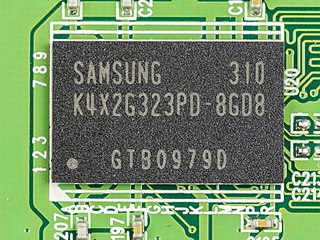
240-pin DDR2 FB-DIMMs are neither mechanically nor electrically compatible with conventional 240-pin DDR2 DIMMs. As a result, those two DIMM types are notched differently to prevent using the wrong one.
As with nearly all RAM specifications, the FB-DIMM specification was published by JEDEC.
Technology
FB-DIMM DDR2 vs DIMM DDR2
Fully buffered DIMM architecture introduces an advanced memory buffer (AMB) between the memory controller and the memory module. Unlike the parallel bus architecture of traditional DRAMs, an FB-DIMM has a serial interface between the memory controller and the AMB. This enables an increase to the width of the memory without increasing the pin count of the memory controller beyond a feasible level. With this architecture, the memory controller does not write to the memory module directly; rather it is done via the AMB. AMB can thus compensate for signal deterioration by buffering and resending the signal.
The AMB can also offer error correction, without imposing any additional overhead on the processor or the system's memory controller. It can also use the Bit Lane Failover Correction feature to identify bad data paths and remove them from operation, which dramatically reduces command/address errors. Also, since reads and writes are buffered, they can be done in parallel by the memory controller. This allows simpler interconnects, and (in theory) hardware-agnostic memory controller chips (such as DDR2 and DDR3) that can be used interchangeably.
The downsides to this approach are; it introduces latency to the memory request, it requires additional power consumption for the buffer chips, and current implementations create a memory write bus significantly narrower than the memory read bus. This means workloads that use many writes (such as high-performance computing) will be significantly slowed. However, this slowdown is nowhere near as bad as not having enough memory capacity to avoid using significant amounts of virtual memory, so workloads that use extreme amounts of memory in irregular patterns might be helped by using fully buffered DIMMs.[citation needed]
Protocol
The JEDEC standard JESD206 defines the protocol, and JESD82-20 defines the AMB interface to DDR2 memory. The protocol is more generally described in many other places.[1][2][3][4][5] The FB-DIMM channel consists of 14 "northbound" bit lanes carrying data from memory to the processor and 10 "southbound" bit lanes carrying commands and data from the processor to memory. Each bit is carried over a differential pair, clocked at 12 times the basic memory clock rate, 6 times the double-pumped data rate. E.g. for DDR2-667 DRAM chips, the channel would operate at 4000MHz. Every 12 cycles constitute one frame, 168 bits northbound and 120 bits southbound.
One northbound frame carries 144 data bits, the amount of data produced by a 72-bit wide DDR SDRAM array in that time, and 24 bits of CRC for error detection. There is no header information, although unused frames include a deliberately invalid CRC.
One southbound frame carries 98 payload bits and 22 CRC bits. Two payload bits are a frame type, and 24 bits are a command. The remaining 72 bits may be either (depending on the frame type), 72 bits of write data, two more 24-bit commands, or one more command plus 36 bits of data to be written to an AMB control register.
The commands correspond to standard DRAM access cycles, such as row select, precharge, and refresh commands. Read and write commands include only column addresses. All commands include a 3-bit FB-DIMM address, allowing up to 8 FB-DIMM modules on a channel.
Because write data is supplied more slowly than DDR memory expects it, writes are buffered in the AMB until they can be written in a burst. Write commands are not directly linked to the write data; instead, each AMB has a write data FIFO that is filled by four consecutive write data frames, and is emptied by a write command.
Both northbound and southbound links can operate at full speed with one bit line disabled, by discarding 12 bits of CRC information per frame.
Note that the bandwidth of an FB-DIMM channel is equal to the peak read bandwidth of a DDR memory channel (and this speed can be sustained, as there is no contention for the northbound channel), plus half of the peak write bandwidth of a DDR memory channel (which can often be sustained, if one command per frame is sufficient). The only overhead is the need for a channel sync frame (which elicits a northbound status frame in response) every 32 to 42 frames (2.5–3% overhead).
Implementations
Intel has adopted the technology for their Xeon 5000/5100 series and beyond, which they consider "a long-term strategic direction for servers".[6]
Intel's enthusiast system platform Skulltrail uses FB-DIMMs for their dual CPU socket, multi-GPU system.[8]
FB-DIMMS have 240 pins and are the same total length as other DDR DIMMs but differ by having indents on both ends within the slot.
The cost of FB-DIMM memory was initially much higher than registered DIMM, which may be one of the factors behind its current level of acceptance. Also, the AMB chip dissipates considerable heat, leading to additional cooling problems. Although strenuous efforts were made to minimize delay in the AMB, there is some noticeable cost in memory access latency.[9][10][11]
History
As of September 2006, AMD has taken FB-DIMM off their roadmap.[12] In December 2006, AMD has revealed in one of the slides that microprocessors based on the new K10 microarchitecture has the support for FB-DIMM "when appropriate".[13] In addition, AMD also developed Socket G3 Memory Extender (G3MX), which uses a single buffer for every 4 modules instead of one for each, to be used by Opteron-based systems in 2009.[14]
At the 2007 Intel Developer Forum, it was revealed that major memory manufacturers have no plans to extend FB-DIMM to support DDR3 SDRAM. Instead, only registered DIMM for DDR3 SDRAM had been demonstrated.[15]
In 2007, Intel demonstrated FB-DIMM with shorter latencies, CL5 and CL3, showing improvement in latencies.[16]
On August 5, 2008, Elpida Memory announced that it would mass-produce the world's first FB-DIMM at 16 Gigabyte capacity, as from Q4 2008,[17] however as of January2011[update] the product has not appeared and the press release has been deleted from Elpida's site.[18]
Double Data Rate Synchronous Dynamic Random-Access Memory is a double data rate (DDR) synchronous dynamic random-access memory (SDRAM) class of memory integrated circuits used in computers. DDR SDRAM, also retroactively called DDR1 SDRAM, has been superseded by DDR2 SDRAM, DDR3 SDRAM, DDR4 SDRAM and DDR5 SDRAM. None of its successors are forward or backward compatible with DDR1 SDRAM, meaning DDR2, DDR3, DDR4 and DDR5 memory modules will not work on DDR1-equipped motherboards, and vice versa.
Synchronous dynamic random-access memory is any DRAM where the operation of its external pin interface is coordinated by an externally supplied clock signal.
A DIMM, or Dual In-Line Memory Module, is a type of computer memory module used in desktop, laptop, and server computers. It is a circuit board that contains memory chips and connects to the computer's motherboard. A DIMM is often called a "RAM stick" due to its shape and size. A DIMM comprises a series of dynamic random-access memory integrated circuits that are mounted to its circuit board. DIMMs are the predominant method for adding memory into a computer system. The vast majority of DIMMs are standardized through JEDEC standards, although there are proprietary DIMMs. DIMMs come in a variety of speeds and sizes, but generally are one of two lengths - PC which are 133.35 mm (5.25 in) and laptop (SO-DIMM) which are about half the size at 67.60 mm (2.66 in).
Rambus DRAM (RDRAM), and its successors Concurrent Rambus DRAM (CRDRAM) and Direct Rambus DRAM (DRDRAM), are types of synchronous dynamic random-access memory (SDRAM) developed by Rambus from the 1990s through to the early 2000s. The third-generation of Rambus DRAM, DRDRAM was replaced by XDR DRAM. Rambus DRAM was developed for high-bandwidth applications and was positioned by Rambus as replacement for various types of contemporary memories, such as SDRAM.
Double Data Rate 2 Synchronous Dynamic Random-Access Memory is a double data rate (DDR) synchronous dynamic random-access memory (SDRAM) interface. It is a JEDEC standard (JESD79-2); first published in September 2003. DDR2 succeeded the original DDR SDRAM specification, and was itself succeeded by DDR3 SDRAM in 2007. DDR2 DIMMs are neither forward compatible with DDR3 nor backward compatible with DDR.
In computing, double data rate (DDR) describes a computer bus that transfers data on both the rising and falling edges of the clock signal. This is also known as double pumped, dual-pumped, and double transition. The term toggle mode is used in the context of NAND flash memory.
In the fields of digital electronics and computer hardware, multi-channel memory architecture is a technology that increases the data transfer rate between the DRAM memory and the memory controller by adding more channels of communication between them. Theoretically, this multiplies the data rate by exactly the number of channels present. Dual-channel memory employs two channels. The technique goes back as far as the 1960s having been used in IBM System/360 Model 91 and in CDC 6600.
Registered memory is computer memory that has a register between the DRAM modules and the system's memory controller. A registered memory module places less electrical load on a memory controller compared to an unregistered one. Registered memory allows a computer system to remain stable with a higher number of memory modules than it would have otherwise.
The AMD Family 10h, or K10, is a microprocessor microarchitecture by AMD based on the K8 microarchitecture. The first third-generation Opteron products for servers were launched on September 10, 2007, with the Phenom processors for desktops following and launching on November 11, 2007 as the immediate successors to the K8 series of processors.
In computing, serial presence detect (SPD) is a standardized way to automatically access information about a memory module. Earlier 72-pin SIMMs included five pins that provided five bits of parallel presence detect (PPD) data, but the 168-pin DIMM standard changed to a serial presence detect to encode more information.
Double Data Rate 3 Synchronous Dynamic Random-Access Memory is a type of synchronous dynamic random-access memory (SDRAM) with a high bandwidth interface, and has been in use since 2007. It is the higher-speed successor to DDR and DDR2 and predecessor to DDR4 synchronous dynamic random-access memory (SDRAM) chips. DDR3 SDRAM is neither forward nor backward compatible with any earlier type of random-access memory (RAM) because of different signaling voltages, timings, and other factors.
Memory bandwidth is the rate at which data can be read from or stored into a semiconductor memory by a processor. Memory bandwidth is usually expressed in units of bytes/second, though this can vary for systems with natural data sizes that are not a multiple of the commonly used 8-bit bytes.
A memory controller is a digital circuit that manages the flow of data going to and from a computer's main memory. A memory controller can be a separate chip or integrated into another chip, such as being placed on the same die or as an integral part of a microprocessor; in the latter case, it is usually called an integrated memory controller (IMC). A memory controller is sometimes also called a memory chip controller (MCC) or a memory controller unit (MCU).
Graphics Double Data Rate 5 Synchronous Dynamic Random-Access Memory is a type of synchronous graphics random-access memory (SGRAM) with a high bandwidth interface designed for use in graphics cards, game consoles, and high-performance computing. It is a type of GDDR SDRAM.
The Socket G3 Memory Extender (G3MX) was a planned Advanced Micro Devices' solution to the problem of connecting large amounts of memory to a single microprocessor. The G3MX was expected to be available on AMD 800S series chipset for server market starting from 2009, but was officially cancelled together with the cancellation of Socket G3 in early 2008.
Double Data Rate 4 Synchronous Dynamic Random-Access Memory is a type of synchronous dynamic random-access memory with a high bandwidth interface.
Low-Power Double Data Rate (LPDDR), also known as LPDDR SDRAM, is a type of synchronous dynamic random-access memory that consumes less power and is targeted for mobile computers and devices such as mobile phones. Older variants are also known as Mobile DDR, and abbreviated as mDDR.
A memory rank is a set of DRAM chips connected to the same chip select, which are therefore accessed simultaneously. In practice all DRAM chips share all of the other command and control signals, and only the chip select pins for each rank are separate.
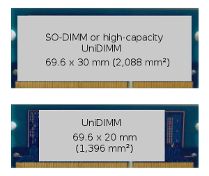
UniDIMM is a specification for dual in-line memory modules (DIMMs), which are printed circuit boards (PCBs) designed to carry dynamic random-access memory (DRAM) chips. UniDIMMs can be populated with either DDR3 or DDR4 chips, with no support for any additional memory control logic; as a result, the computer's memory controller must support both DDR3 and DDR4 memory standards. The UniDIMM specification was created by Intel for its Skylake microarchitecture, whose integrated memory controller (IMC) supports both DDR3 and DDR4 memory technologies.
This page is based on this Wikipedia article Text is available under the CC BY-SA 4.0 license; additional terms may apply. Images, videos and audio are available under their respective licenses.