Related Research Articles
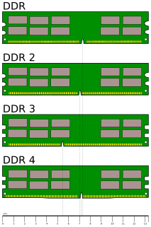
Double Data Rate Synchronous Dynamic Random-Access Memory, officially abbreviated as DDR SDRAM, is a double data rate (DDR) synchronous dynamic random-access memory (SDRAM) class of memory integrated circuits used in computers. DDR SDRAM, also retroactively called DDR1 SDRAM, has been superseded by DDR2 SDRAM, DDR3 SDRAM and DDR4 SDRAM. None of its successors are forward or backward compatible with DDR1 SDRAM, meaning DDR2, DDR3, and DDR4 memory modules will not work in DDR1-equipped motherboards, and vice versa.

A DIMM or dual in-line memory module comprises a series of dynamic random-access memory integrated circuits. These modules are mounted on a printed circuit board and designed for use in personal computers, workstations and servers. DIMMs began to replace SIMMs as the predominant type of memory module as Intel P5-based Pentium processors began to gain market share.
Rambus DRAM (RDRAM), and its successors Concurrent Rambus DRAM (CRDRAM) and Direct Rambus DRAM (DRDRAM), are types of synchronous dynamic random-access memory (SDRAM) developed by Rambus from the 1990s through to the early-2000s. The third-generation of Rambus DRAM, DRDRAM was replaced by XDR DRAM. Rambus DRAM was developed for high-bandwidth applications, and was positioned by Rambus as replacement for various types of contemporary memories, such as SDRAM.
HyperTransport (HT), formerly known as Lightning Data Transport (LDT), is a technology for interconnection of computer processors. It is a bidirectional serial/parallel high-bandwidth, low-latency point-to-point link that was introduced on April 2, 2001. The HyperTransport Consortium is in charge of promoting and developing HyperTransport technology.

A front-side bus (FSB) is a computer communication interface (bus) that was often used in Intel-chip-based computers during the 1990s and 2000s. The EV6 bus served the same function for competing AMD CPUs. Both typically carry data between the central processing unit (CPU) and a memory controller hub, known as the northbridge.
The Athlon 64 is an eighth-generation, AMD64-architecture microprocessor produced by AMD, released on September 23, 2003. It is the third processor to bear the name Athlon, and the immediate successor to the Athlon XP. The second processor to implement AMD64 architecture and the first 64-bit processor targeted at the average consumer, it was AMD's primary consumer microprocessor, and competes primarily with Intel's Pentium 4, especially the "Prescott" and "Cedar Mill" core revisions. It is AMD's first K8, eighth-generation processor core for desktop and mobile computers. Despite being natively 64-bit, the AMD64 architecture is backward-compatible with 32-bit x86 instructions. Athlon 64s have been produced for Socket 754, Socket 939, Socket 940 and Socket AM2. The line was succeeded by the dual-core Athlon 64 X2 and Athlon X2 lines.

Xeon is a brand of x86 microprocessors designed, manufactured, and marketed by Intel, targeted at the non-consumer workstation, server, and embedded system markets. It was introduced in June 1998. Xeon processors are based on the same architecture as regular desktop-grade CPUs, but have some advanced features such as support for ECC memory, higher core counts, support for larger amounts of RAM, larger cache memory and extra provision for enterprise-grade reliability, availability and serviceability (RAS) features responsible for handling hardware exceptions through the Machine Check Architecture. They are often capable of safely continuing execution where a normal processor cannot due to these extra RAS features, depending on the type and severity of the machine-check exception (MCE). Some also support multi-socket systems with two, four, or eight sockets through use of the Quick Path Interconnect (QPI) bus.

Double Data Rate 2 Synchronous Dynamic Random-Access Memory, officially abbreviated as DDR2 SDRAM, is a double data rate synchronous dynamic random-access memory interface. It superseded the original DDR SDRAM specification, and is superseded by DDR3 SDRAM. DDR2 DIMMs are neither forward compatible with DDR3 nor backward compatible with DDR.

A northbridge or host bridge is one of the two chips in the core logic chipset architecture on a PC motherboard, the other being the southbridge. Unlike the southbridge, northbridge is connected directly to the CPU via the front-side bus (FSB) and is thus responsible for tasks that require the highest performance. The northbridge, also known as Memory Controller Hub, is usually paired with a southbridge. In systems where they are included, these two chips manage communications between the CPU and other parts of the motherboard, and constitute the core logic chipset of the PC motherboard.
In the fields of digital electronics and computer hardware, multi-channel memory architecture is a technology that increases the data transfer rate between the DRAM memory and the memory controller by adding more channels of communication between them. Theoretically this multiplies the data rate by exactly the number of channels present. Dual-channel memory employs two channels. The technique goes back as far as the 1960s having been used in IBM System/360 Model 91 and in CDC 6600.
The AMD Family 10h, or K10, is a microprocessor microarchitecture by AMD based on the K8 microarchitecture. Though there were once reports that the K10 had been canceled, the first third-generation Opteron products for servers were launched on September 10, 2007, with the Phenom processors for desktops following and launching on November 11, 2007 as the immediate successors to the K8 series of processors.
Double Data Rate 3 Synchronous Dynamic Random-Access Memory, officially abbreviated as DDR3 SDRAM, is a type of synchronous dynamic random-access memory (SDRAM) with a high bandwidth interface, and has been in use since 2007. It is the higher-speed successor to DDR and DDR2 and predecessor to DDR4 synchronous dynamic random-access memory (SDRAM) chips. DDR3 SDRAM is neither forward nor backward compatible with any earlier type of random-access memory (RAM) because of different signaling voltages, timings, and other factors.

Fully Buffered DIMM is a memory technology that can be used to increase reliability and density of memory systems. Conventionally, data lines from the memory controller have to be connected to data lines in every DRAM module, i.e. via multidrop buses. As the memory width increases together with the access speed, the signal degrades at the interface between the bus and the device. This limits the speed and memory density, so FB-DIMMs take a different approach to solve the problem.
The memory controller is a digital circuit that manages the flow of data going to and from the computer's main memory. A memory controller can be a separate chip or integrated into another chip, such as being placed on the same die or as an integral part of a microprocessor; in the latter case, it is usually called an integrated memory controller (IMC). A memory controller is sometimes also called a memory chip controller (MCC) or a memory controller unit (MCU).
The P35 Express is a mainstream desktop computer chipset from Intel released in June 2007, although motherboards featuring the chipset were available a month earlier. The P35 Express chipset supports Intel's LGA 775 socket and Core 2 Duo and Quad processors, and is also known to support 45 nm Wolfdale/Yorkfield dual and quad core CPUs. Theoretically, Intel also dropped support for Intel's Pentium 4 and Pentium D processors with this chipset although late Pentium 4 processors, including both the 32-bit-only (5x0) and the 32-bit/64-bit (5x1), and a few others, were fully supported.
Double Data Rate 4 Synchronous Dynamic Random-Access Memory, officially abbreviated as DDR4 SDRAM, is a type of synchronous dynamic random-access memory with a high bandwidth interface.
Apollo VP3 is a x86 based Socket 7 chipset which was manufactured by VIA Technologies and was launched in 1997. On its time Apollo VP3 was a high performance, cost effective, and energy efficient chipset. It offered AGP support for Socket 7 processors which was not supported at that moment by Intel, SiS and ALi chipsets. In November 1997 FIC released motherboard PA-2012, which uses Apollo VP3 and has AGP bus. This was the first Socket 7 motherboard supporting AGP.

LGA 1151, also known as Socket H4, is an Intel microprocessor compatible socket which comes in two distinct versions: the first revision which supports both Intel's Skylake and Kaby Lake CPUs, and the second revision which supports Coffee Lake CPUs exclusively.
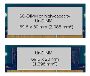
UniDIMM is a specification for dual in-line memory modules (DIMMs), which are printed circuit boards (PCBs) designed to carry dynamic random-access memory (DRAM) chips. UniDIMMs can be populated with either DDR3 or DDR4 chips, with no support for any additional memory control logic; as a result, the computer's memory controller must support both DDR3 and DDR4 memory standards. The UniDIMM specification was created by Intel for its Skylake microarchitecture, whose integrated memory controller (IMC) supports both DDR3 and DDR4 memory technologies.
References
- "AMD Unveils Forward-Looking Technology Innovation To Extend Memory Footprint for Server Computing" (Press release). Advanced Micro Devices. 2007-07-25. Retrieved 2007-10-07.
- Shaun Nichols (2007-07-25). "AMD claims memory controller breakthrough". California: vnunet.com. Retrieved 2007-10-07.
- Marco Chiappetta (2007-08-22). "More AMD G3MX Details Emerge". HotHardware. Retrieved 2007-10-07. Also mentions rumors that Intel is working on a similar on-motherboard "AMB2".
- ↑ (in Japanese) PC Watch report, retrieved August 20, 2008