
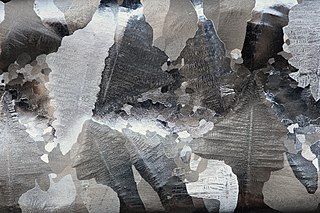
Anisotropy is the structural property of non-uniformity in different directions, as opposed to isotropy. An anisotropic object or pattern has properties that differ according to direction of measurement. For example, many materials exhibit very different physical or mechanical properties when measured along different axes, e.g. absorbance, refractive index, conductivity, and tensile strength.

In physics and geometry, isotropy is uniformity in all orientations. Precise definitions depend on the subject area. Exceptions, or inequalities, are frequently indicated by the prefix a- or an-, hence anisotropy. Anisotropy is also used to describe situations where properties vary systematically, dependent on direction. Isotropic radiation has the same intensity regardless of the direction of measurement, and an isotropic field exerts the same action regardless of how the test particle is oriented.

MEMS is the technology of microscopic devices incorporating both electronic and moving parts. MEMS are made up of components between 1 and 100 micrometres in size, and MEMS devices generally range in size from 20 micrometres to a millimetre, although components arranged in arrays can be more than 1000 mm2. They usually consist of a central unit that processes data and several components that interact with the surroundings.

Semiconductor device fabrication is the process used to manufacture semiconductor devices, typically integrated circuits (ICs) such as computer processors, microcontrollers, and memory chips. It is a multiple-step photolithographic and physico-chemical process during which electronic circuits are gradually created on a wafer, typically made of pure single-crystal semiconducting material. Silicon is almost always used, but various compound semiconductors are used for specialized applications.

Epitaxy refers to a type of crystal growth or material deposition in which new crystalline layers are formed with one or more well-defined orientations with respect to the crystalline seed layer. The deposited crystalline film is called an epitaxial film or epitaxial layer. The relative orientation(s) of the epitaxial layer to the seed layer is defined in terms of the orientation of the crystal lattice of each material. For most epitaxial growths, the new layer is usually crystalline and each crystallographic domain of the overlayer must have a well-defined orientation relative to the substrate crystal structure. Epitaxy can involve single-crystal structures, although grain-to-grain epitaxy has been observed in granular films. For most technological applications, single-domain epitaxy, which is the growth of an overlayer crystal with one well-defined orientation with respect to the substrate crystal, is preferred. Epitaxy can also play an important role while growing superlattice structures.
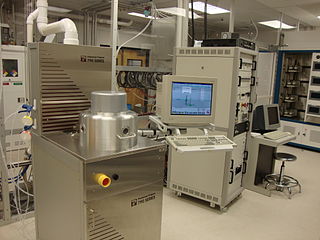
Reactive-ion etching (RIE) is an etching technology used in microfabrication. RIE is a type of dry etching which has different characteristics than wet etching. RIE uses chemically reactive plasma to remove material deposited on wafers. The plasma is generated under low pressure (vacuum) by an electromagnetic field. High-energy ions from the plasma attack the wafer surface and react with it.
Dry etching refers to the removal of material, typically a masked pattern of semiconductor material, by exposing the material to a bombardment of ions that dislodge portions of the material from the exposed surface. A common type of dry etching is reactive-ion etching. Unlike with many of the wet chemical etchants used in wet etching, the dry etching process typically etches directionally or anisotropically.
Surface micromachining builds microstructures by deposition and etching structural layers over a substrate. This is different from Bulk micromachining, in which a silicon substrate wafer is selectively etched to produce structures.
Bulk micromachining is a process used to produce micromachinery or microelectromechanical systems (MEMS).
Deep reactive-ion etching (DRIE) is a special subclass of reactive-ion etching (RIE). It enables highly anisotropic etch process used to create deep penetration, steep-sided holes and trenches in wafers/substrates, typically with high aspect ratios. It was developed for microelectromechanical systems (MEMS), which require these features, but is also used to excavate trenches for high-density capacitors for DRAM and more recently for creating through-silicon vias (TSVs) in advanced 3D wafer level packaging technology.
Plasma etching is a form of plasma processing used to fabricate integrated circuits. It involves a high-speed stream of glow discharge (plasma) of an appropriate gas mixture being shot at a sample. The plasma source, known as etch species, can be either charged (ions) or neutral. During the process, the plasma generates volatile etch products at room temperature from the chemical reactions between the elements of the material etched and the reactive species generated by the plasma. Eventually the atoms of the shot element embed themselves at or just below the surface of the target, thus modifying the physical properties of the target.

Xenon difluoride is a powerful fluorinating agent with the chemical formula XeF
2, and one of the most stable xenon compounds. Like most covalent inorganic fluorides it is moisture-sensitive. It decomposes on contact with water vapor, but is otherwise stable in storage. Xenon difluoride is a dense, colourless crystalline solid.

Etching is used in microfabrication to chemically remove layers from the surface of a wafer during manufacturing. Etching is a critically important process module in fabrication, and every wafer undergoes many etching steps before it is complete.

Hexafluoroethane is the perfluorocarbon counterpart to the hydrocarbon ethane. It is a non-flammable gas negligibly soluble in water and slightly soluble in methanol. It is an extremely potent and long-lived greenhouse gas.

The Wright etch is a preferential etch for revealing defects in <100>- and <111>-oriented, p- and n-type silicon wafers used for making transistors, microprocessors, memories, and other components. Revealing, identifying, and remedying such defects is essential for progress along the path predicted by Moore's law. It was developed by Margaret Wright Jenkins (1936-2018) in 1976 while working in research and development at Motorola Inc. in Phoenix, AZ. It was published in 1977. This etchant reveals clearly defined oxidation-induced stacking faults, dislocations, swirls and striations with minimum surface roughness or extraneous pitting. These defects are known causes of shorts and current leakage in finished semiconductor devices should they fall across isolated junctions. A relatively low etch rate at room temperature provides etch control. The long shelf life of this etchant allows the solution to be stored in large quantities.

Photolithography is a process in removing select portions of thin films used in microfabrication. Microfabrication is the production of parts on the micro- and nano- scale, typically on the surface of silicon wafers, for the production of integrated circuits, microelectromechanical systems (MEMS), solar cells, and other devices. Photolithography makes this process possible through the combined use of hexamethyldisilazane (HMDS), photoresist, spin coating, photomask, an exposure system and other various chemicals. By carefully manipulating these factors it is possible to create nearly any geometry microstructure on the surface of a silicon wafer. The chemical interaction between all the different components and the surface of the silicon wafer makes photolithography an interesting chemistry problem. Current engineering has been able to create features on the surface of silicon wafers between 1 and 100 μm.
Chemical milling or industrial etching is the subtractive manufacturing process of using baths of temperature-regulated etching chemicals to remove material to create an object with the desired shape. Other names for chemical etching include photo etching, chemical etching, photo chemical etching and photochemical machining. It is mostly used on metals, though other materials are increasingly important. It was developed from armor-decorating and printing etching processes developed during the Renaissance as alternatives to engraving on metal. The process essentially involves bathing the cutting areas in a corrosive chemical known as an etchant, which reacts with the material in the area to be cut and causes the solid material to be dissolved; inert substances known as maskants are used to protect specific areas of the material as resists.
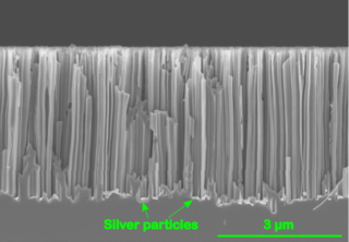
Metal Assisted Chemical Etching is the process of wet chemical etching of semiconductors with the use of a metal catalyst, usually deposited on the surface of a semiconductor in the form of a thin film or nanoparticles. The semiconductor, covered with the metal is then immersed in an etching solution containing and oxidizing agent and hydrofluoric acid. The metal on the surface catalyzes the reduction of the oxidizing agent and therefore in turn also the dissolution of silicon. In the majority of the conducted research this phenomenon of increased dissolution rate is also spatially confined, such that it is increased in close proximity to a metal particle at the surface. Eventually this leads to the formation of straight pores that are etched into the semiconductor. This means that a pre-defined pattern of the metal on the surface can be directly transferred to a semiconductor substrate.
Vapor etching refers to a process used in the fabrication of Microelectromechanical systems (MEMS) and Nanoelectromechanical systems (NEMS). Sacrificial layers are isotropically etched using gaseous acids such as Hydrogen fluoride and Xenon difluoride to release the free standing components of the device.

Undercuts from etching (microfabrication) are generally an unwanted side effect, however are sometimes used as a feature such as in the Niemeyer–Dolan technique. Undercuts from etching can occur from two common causes. The first is over etching, which means the etchant was applied too long. The second is due to an isotropic etchant, which means the etchant etches in all directions equally. To overcome this problem an anisotropic etchant is used.